LordOfChaos
Member
Intel has a long history of making integrated GPUs, and they've recognized how important iGPUs are to thin and light laptops. Today Intel is locked in fierce competition with AMD, and the company's fight to hold on to the laptop market is no less intense on the graphics front. Lunar Lake is Intel's latest mobile offering, and brings with it a new Xe2 graphics architecture. Xe2 is an evolution of the Xe-LPG/HPG architectures used on the outgoing Meteor Lake mobile chips and Intel's current Arc discrete GPUs. It aims to better fit expected workloads and improve efficiency, and will be used across both Lunar Lake and Intel's upcoming "Battlemage" discrete GPUs.

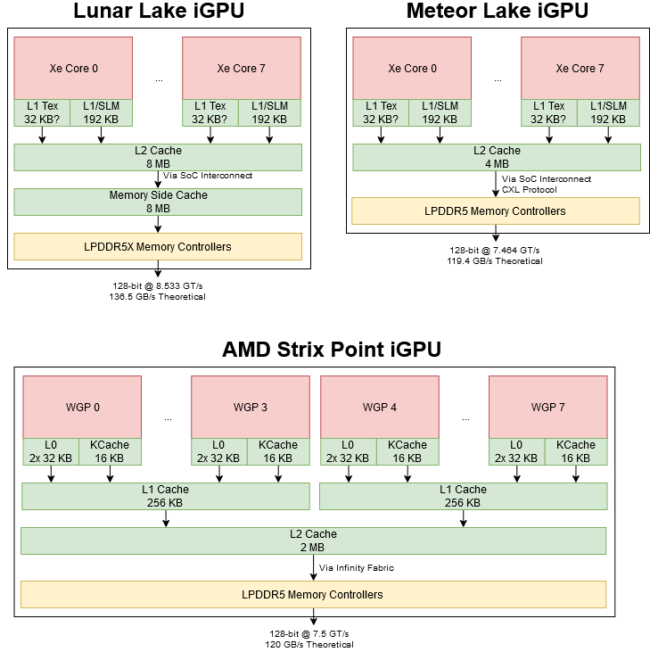
Modern GPUs are modular, scalable designs and Intel's Xe2 is no different. An Xe2 iGPU is built from Xe Cores, much like how AMD's RDNA GPUs are built from WGPs (Workgroup Processors) or how Nvidia's GPUs are built from SMs (Streaming Multiprocessors). Lunar Lake's iGPU features eight Xe Cores, further divided into two Render Slices with four Xe Cores each. These Render Slices include fixed function graphics hardware like a rasterizer and pixel backends (ROPs). Lunar Lake's iGPU is therefore laid out similarly to Meteor Lake's iGPU, which also has eight Xe Cores split across two Render Slices.

Intel's Render Slice vaguely corresponds to AMD's Shader Array, which also includes a rasterizer and ROPs. AMD also has a mid-level L1 cache at the Shader Array level, with 256 KB of capacity on RDNA 3.5. Intel also has caches at the Render Slice level, though only for fixed function graphics hardware. The figure below should be taken with a grain of salt because Intel has not published documentation for Xe-LPG, so I'm taking figures from the closely related Xe-HPG. I also find Intel's documentation confusing. For example, each pixel backend should have its own color cache, but something changed after Tiger Lake and Intel only documents one color cache instance per slice despite drawing it twice in other diagrams.
More at the link

 chipsandcheese.com

Modern GPUs are modular, scalable designs and Intel's Xe2 is no different. An Xe2 iGPU is built from Xe Cores, much like how AMD's RDNA GPUs are built from WGPs (Workgroup Processors) or how Nvidia's GPUs are built from SMs (Streaming Multiprocessors). Lunar Lake's iGPU features eight Xe Cores, further divided into two Render Slices with four Xe Cores each. These Render Slices include fixed function graphics hardware like a rasterizer and pixel backends (ROPs). Lunar Lake's iGPU is therefore laid out similarly to Meteor Lake's iGPU, which also has eight Xe Cores split across two Render Slices.

Intel's Render Slice vaguely corresponds to AMD's Shader Array, which also includes a rasterizer and ROPs. AMD also has a mid-level L1 cache at the Shader Array level, with 256 KB of capacity on RDNA 3.5. Intel also has caches at the Render Slice level, though only for fixed function graphics hardware. The figure below should be taken with a grain of salt because Intel has not published documentation for Xe-LPG, so I'm taking figures from the closely related Xe-HPG. I also find Intel's documentation confusing. For example, each pixel backend should have its own color cache, but something changed after Tiger Lake and Intel only documents one color cache instance per slice despite drawing it twice in other diagrams.
More at the link

Lunar Lake’s iGPU: Debut of Intel’s Xe2 Architecture
Intel has a long history of making integrated GPUs, and they’ve recognized how important iGPUs are to thin and light laptops.
