midnightguy
Member
http://www.tinyurl.com/9k8f8
Hiroshige's Goto Weekly overseas news
Graphic engine RSX of PLAYSTATION
- As for RSX and G70 GPU
The SONY * computer entertainment (the SCEI) the NVIDIA it developed the GPU which is loaded onto the next generation machine " PLAYSTATION 3 ", " the RSX (the Reality Synthesizer)". This RSX, is presumed up-to-date high ended GPU " GeForce 7800 GTX of the NVIDIA (the G70)" with, it is the GPU of the twins.
The David B Kirk person of the NVIDIA (the Chief Scientist), concerning both GPU " Shader architecture of the RSX, the G70 is designated as the base ", it has explained. Perhaps, the difference of the RSX and the G70, is seen it is no more than a process technology and the system bus, and memory interface width. G70 with 0.11 mu m process of TSMC PCI Express x16, GDDR3 interface of 256bit width. RSX with the SONY / Toshiba 90nm process FlexcIo (Redwood: Redwood) with, memory interface of 128bit width. Concerning the Shader constitution the other than that and the micro architecture et cetera of the Shader, the difference is presumed in both GPU almost it is not.
RSX Block Diagram
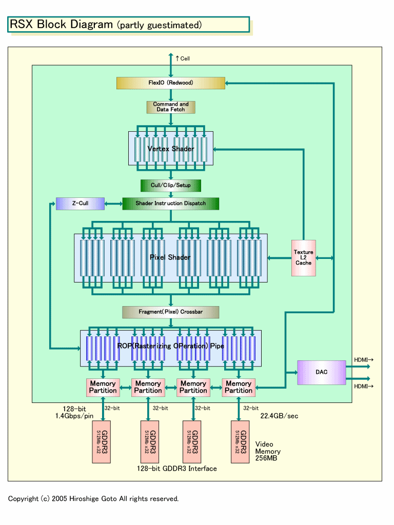
( it is not the official block diagram of RSX but one based heavily on G70)
As for the reason which you think there is no difference in Shader constitution, it is several, but as for largest basis there are announcement specifications with the E3. When it becomes 136 Shader Operations/cycle, concerning the parallel characteristic of the Shader of the RSX, it explained the NVIDIA, with the E3.
These specifications are presumed the Xbox 360 GPU of the ATI development which the Microsoft announces (the R500) opposing to the specifications, those which are published. As for the Microsoft, Shader operation efficiency of the Xbox 360 GPU has published, 48 billion shader operations/sec, when it converts, 96 Shader Operations/cycle (it divides) with it becomes with the 500MHz. The numerical value which is higher than that as the NVIDIA which does specifications competition, was shown, you probably apply.
However, the " Shader Operations/sec " in expression of the ATI, with NVIDIA inscription is suitable to the Instructions/sec almost. The NVIDIA has counted the plural operations which issue in 1 order, as the Operations/sec because parallel characteristic of order issue has counted as another specifications. The specifications at the time of the E3 are seen because the NVIDIA opposes to the ATI, transitory inscription was fitted.
With being the case that it is said, 136 Shader Operations/cycle of the RSX, are presumed with original inscription of the NVIDIA it becomes 136 Instructions/cycle. So, this being what specifications? As for the Vertex Shader of G70 type 2 Instructions/cycle, as for the Pixel Shader when it has the parallel characteristic of order issue of 5 Instructions/cycle, it has explained the NVIDIA. Because of that, when constitution of the G70 (Vertex Shader 8/Pixel Shader 24) is, it is published altogether GPU it becomes 136 Instructions/cycle.
In other words, if you look at the specifications of the Instructions/cycle, it can presume the Shader constitution of the G70 and the RSX completely it is the same. Also the RSX, when we assume the Vertex Shader 8 units, the Pixel Shader with constitution of 24 units, has the mechanism of the same order issue as the respective G70, becomes these specifications.
Actually, as for the person who says that the G70 and the RSX almost are identical architecture, it is many in the GPU industry authorized personnel. As for a certain authorized personnel " as for the NVIDIA finally concluding contract with the SCEI around summer of 2004 was. Therefore, as for the NVIDIA there was no enough time which develops the architecture which customizes in for the SCEI ", that.
It can presume that almost probably there is no difference in constitution of both GPU, even from the number of transistors. As for the number of transistors, the G70 is announced 3 hundred million 200 ten thousand (302m), the RSX 3 hundred million (300M) or more. The PCI Express x16 as for mounting is heavier than the FlexcIo, when you think of that also the DRAM controller is 2 times, you can agree upon this difference.
- As for Shader operational performance of RSX 28% increase
Shader architecture of the G70, GeForce 6800 (NV40) in the base, strengthened the parallel characteristic inside the especially Pixel Shader. For example, with the NV40, it has two vectoring operational units inside the Pixel Shader, but vectoring unit of one side could not do 1 cycle throughput sum of products calculation. With the G70 it is designed in such a way that it can do product-sum operation. The figure under the block diagram inside the Shader of the G70 is, but it is presumed also the RSX almost is the same as this.
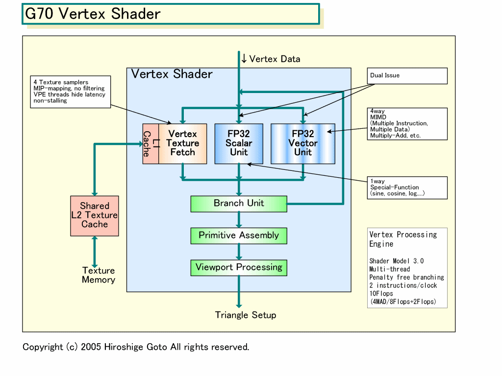
G70 Vertex Shader
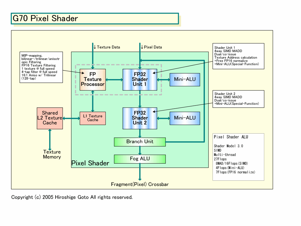
G70 Pixel Shader
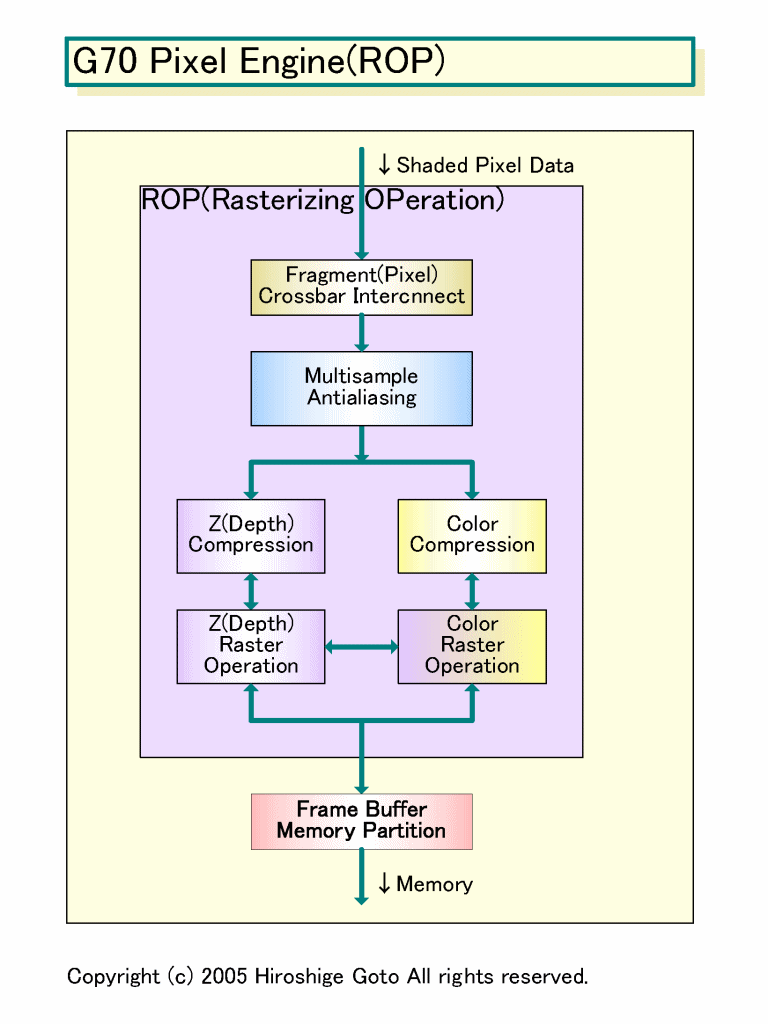
G70 Pixel Shader (ROP)
Assuming, Shader architecture of the G70 and the RSX is the same, operational performance differs largely. Because as for that operational frequency is different. As for the present G70 as for the product specifications as for the RSX the 550MHz is planned the 430MHz, vis-a-vis that. As for frequency because about 28% the RSX is higher, with peak operational efficiency with respect to theory as for the RSX it reaches 1.28 times that the G70.
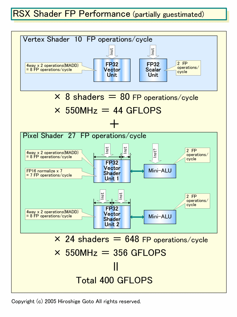
With the specifications of the G70 which the NVIDIA is open, the Vertex Shader with 4way VLIW unit + 1 scalar unit, can calculate 5 data in parallel. With sum of products calculation, as for floating point operation per 1 cycle 10. Because the Vertex Shader is 8, operational efficiency becomes in regard to calculation, as follows.
(4way+1scalar) X 2 FP operations (MADD) = 10 FP operations/cycle
10 FP operations X 8 Shader X 430MHz = 34.4GFLOPS
As for the Pixel Shader of the G70, you say the scalar operational unit where SIMD unit of the 4way is called 2 units and the Mini-ALU 2, the FP16 normalize of the 7way (formalization) is processing unit. Because of that, operational efficiency becomes like under.
((4way X 2 Units + 2 scalar) X 2 FPoperations) + 7 normalize = 27 FP operations/cycle
27 FP operations X 24 Shader X 430MHz = 278.6GFLOPS
Shader constitution being the same, when we assume, the clock is the 550MHz, operational efficiency of the RSX becomes like below.
Vertex Shader
10 FP operations X 8 Shader X 550MHz = 44GFLOPS
Pixel Shader
27 FP operations X 24 Shader X 550MHz = 356.4GFLOPS
44GFLOPS + 356.4GFLOPS = 400.4GFLOPS
RSX Shader FP Performance
Because the Xbox 360 GPU (the R500) Shader floating point arithmetic efficiency is the 240GFLOPS, in regard to calculation becomes peak Shader floating point arithmetic efficiency of 1.66 times. But, as for the RSX and the Xbox 360 GPU because architecture differs completely, as for actual efficiency it cannot infer simply from this number. To the last, only it is standard of the operational quantity.
- Changes the method of using the GPU broadband
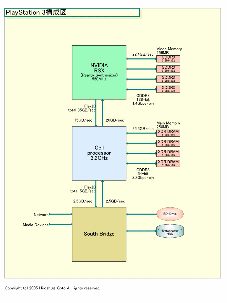
The fact that most it differs in the G70 and the RSX is architecture of the host bus. Vis-a-vis the G70 being the PCI Express x16, as for the RSX the FlexcIo of the Rambus (the Redwood: The redwood) you use. As for zone of the PCI Express x16 the type direction 4gB/sec, being bidirectional, the 8gB/sec. Vis-a-vis that, the FlexcIo descends and (the Cell -> the RSX) rises and the 20GB/sec, (the RSX -> the Cell) zone is thick in the 15gB/sec and far. It is broadband of 4.5 times.
Not only saying, simply the data transfer quantity became large, it has an influence the extreme difference of this zone, on also the something related to CPU between the GPU. Because it reaches the point where it can do more positive role allotment between both processor. The PC graphics where the host bus is limited, the graphics which elementary differs becomes possible. Concerning this, already we would like to explain a little in detail.
There is also an advantage in regard to mounting in the FlexcIo. That the die/di which is possessed (the semiconductor itself) is that zone per area is wide. You do not know mounting the PCI Express of the NVIDIA has occupied some area. But, the tip/chip set vendor authorized personnel in each case points out the area where the PCI Express x16 is enormous is needed. As for the FlexcIo, with 13.1 squares mm, RSX side because interface width becomes narrow, the possibility of becoming small is higher than that even with mounting the Cell side of 96bit width.
By the way, as for the FlexcIo with the parallel interface whose constitution is possible at the 8bit unit, on the specifications transfer rate has become the 6.4gbps. But, the specifications of the PS3, 20GB/sec and the 15gB/sec are not agreeable with this transfer rate. Transfer rate descends with the 5gbps, and at the time of the 32bit and the rising 24bit and calculation is agreeable. Because of that, in the product as for the FlexcIo there is a possibility of being dropped into the transfer rate of the 5gbps. In case of the Cell, when at present, the operational frequency of the CPU and transfer rate of XDR DRAM memory are done, same period drop the CPU clock also transfer rate of the XDR DRAM has fallen. But, the FlexcIo is thought it has become asynchronism.
RSX Shader FP Performance
- Architecture of memory
Another difference is memory interface width. The G70 for the PC has the GDDR3 interface of 256bit width. Vis-a-vis that, the RSX when it calculates backward from memory zone, becomes 128bit width. The memory controller means to have decreased in half. Because memory capacity is the 256MB, the DRAM tip/chip is presumed the x32 item of the 512mbit is 4.
The block diagram of the memory controller of the RSX with presumption, still is not secure. With NV40/G70 architecture, as for the memory controller it has divided into 4 partitions. Each partition is connected to the DRAM controller of 64bit width. The ROP at a time 4 units is connected by the memory (controller) partition of specification, also each partition is connected mutually. The crossbar to connect ROP everything 16 it is not vis-a-vis the memory controller, it is seen by the fact that you connect at 4 ROP units, you design the crossbar easy and efficiently.
Hiroshige's Goto Weekly overseas news
Graphic engine RSX of PLAYSTATION
- As for RSX and G70 GPU
The SONY * computer entertainment (the SCEI) the NVIDIA it developed the GPU which is loaded onto the next generation machine " PLAYSTATION 3 ", " the RSX (the Reality Synthesizer)". This RSX, is presumed up-to-date high ended GPU " GeForce 7800 GTX of the NVIDIA (the G70)" with, it is the GPU of the twins.
The David B Kirk person of the NVIDIA (the Chief Scientist), concerning both GPU " Shader architecture of the RSX, the G70 is designated as the base ", it has explained. Perhaps, the difference of the RSX and the G70, is seen it is no more than a process technology and the system bus, and memory interface width. G70 with 0.11 mu m process of TSMC PCI Express x16, GDDR3 interface of 256bit width. RSX with the SONY / Toshiba 90nm process FlexcIo (Redwood: Redwood) with, memory interface of 128bit width. Concerning the Shader constitution the other than that and the micro architecture et cetera of the Shader, the difference is presumed in both GPU almost it is not.
RSX Block Diagram
( it is not the official block diagram of RSX but one based heavily on G70)
As for the reason which you think there is no difference in Shader constitution, it is several, but as for largest basis there are announcement specifications with the E3. When it becomes 136 Shader Operations/cycle, concerning the parallel characteristic of the Shader of the RSX, it explained the NVIDIA, with the E3.
These specifications are presumed the Xbox 360 GPU of the ATI development which the Microsoft announces (the R500) opposing to the specifications, those which are published. As for the Microsoft, Shader operation efficiency of the Xbox 360 GPU has published, 48 billion shader operations/sec, when it converts, 96 Shader Operations/cycle (it divides) with it becomes with the 500MHz. The numerical value which is higher than that as the NVIDIA which does specifications competition, was shown, you probably apply.
However, the " Shader Operations/sec " in expression of the ATI, with NVIDIA inscription is suitable to the Instructions/sec almost. The NVIDIA has counted the plural operations which issue in 1 order, as the Operations/sec because parallel characteristic of order issue has counted as another specifications. The specifications at the time of the E3 are seen because the NVIDIA opposes to the ATI, transitory inscription was fitted.
With being the case that it is said, 136 Shader Operations/cycle of the RSX, are presumed with original inscription of the NVIDIA it becomes 136 Instructions/cycle. So, this being what specifications? As for the Vertex Shader of G70 type 2 Instructions/cycle, as for the Pixel Shader when it has the parallel characteristic of order issue of 5 Instructions/cycle, it has explained the NVIDIA. Because of that, when constitution of the G70 (Vertex Shader 8/Pixel Shader 24) is, it is published altogether GPU it becomes 136 Instructions/cycle.
In other words, if you look at the specifications of the Instructions/cycle, it can presume the Shader constitution of the G70 and the RSX completely it is the same. Also the RSX, when we assume the Vertex Shader 8 units, the Pixel Shader with constitution of 24 units, has the mechanism of the same order issue as the respective G70, becomes these specifications.
Actually, as for the person who says that the G70 and the RSX almost are identical architecture, it is many in the GPU industry authorized personnel. As for a certain authorized personnel " as for the NVIDIA finally concluding contract with the SCEI around summer of 2004 was. Therefore, as for the NVIDIA there was no enough time which develops the architecture which customizes in for the SCEI ", that.
It can presume that almost probably there is no difference in constitution of both GPU, even from the number of transistors. As for the number of transistors, the G70 is announced 3 hundred million 200 ten thousand (302m), the RSX 3 hundred million (300M) or more. The PCI Express x16 as for mounting is heavier than the FlexcIo, when you think of that also the DRAM controller is 2 times, you can agree upon this difference.
- As for Shader operational performance of RSX 28% increase
Shader architecture of the G70, GeForce 6800 (NV40) in the base, strengthened the parallel characteristic inside the especially Pixel Shader. For example, with the NV40, it has two vectoring operational units inside the Pixel Shader, but vectoring unit of one side could not do 1 cycle throughput sum of products calculation. With the G70 it is designed in such a way that it can do product-sum operation. The figure under the block diagram inside the Shader of the G70 is, but it is presumed also the RSX almost is the same as this.
G70 Vertex Shader
G70 Pixel Shader
G70 Pixel Shader (ROP)
Assuming, Shader architecture of the G70 and the RSX is the same, operational performance differs largely. Because as for that operational frequency is different. As for the present G70 as for the product specifications as for the RSX the 550MHz is planned the 430MHz, vis-a-vis that. As for frequency because about 28% the RSX is higher, with peak operational efficiency with respect to theory as for the RSX it reaches 1.28 times that the G70.
With the specifications of the G70 which the NVIDIA is open, the Vertex Shader with 4way VLIW unit + 1 scalar unit, can calculate 5 data in parallel. With sum of products calculation, as for floating point operation per 1 cycle 10. Because the Vertex Shader is 8, operational efficiency becomes in regard to calculation, as follows.
(4way+1scalar) X 2 FP operations (MADD) = 10 FP operations/cycle
10 FP operations X 8 Shader X 430MHz = 34.4GFLOPS
As for the Pixel Shader of the G70, you say the scalar operational unit where SIMD unit of the 4way is called 2 units and the Mini-ALU 2, the FP16 normalize of the 7way (formalization) is processing unit. Because of that, operational efficiency becomes like under.
((4way X 2 Units + 2 scalar) X 2 FPoperations) + 7 normalize = 27 FP operations/cycle
27 FP operations X 24 Shader X 430MHz = 278.6GFLOPS
Shader constitution being the same, when we assume, the clock is the 550MHz, operational efficiency of the RSX becomes like below.
Vertex Shader
10 FP operations X 8 Shader X 550MHz = 44GFLOPS
Pixel Shader
27 FP operations X 24 Shader X 550MHz = 356.4GFLOPS
44GFLOPS + 356.4GFLOPS = 400.4GFLOPS
RSX Shader FP Performance
Because the Xbox 360 GPU (the R500) Shader floating point arithmetic efficiency is the 240GFLOPS, in regard to calculation becomes peak Shader floating point arithmetic efficiency of 1.66 times. But, as for the RSX and the Xbox 360 GPU because architecture differs completely, as for actual efficiency it cannot infer simply from this number. To the last, only it is standard of the operational quantity.
- Changes the method of using the GPU broadband
The fact that most it differs in the G70 and the RSX is architecture of the host bus. Vis-a-vis the G70 being the PCI Express x16, as for the RSX the FlexcIo of the Rambus (the Redwood: The redwood) you use. As for zone of the PCI Express x16 the type direction 4gB/sec, being bidirectional, the 8gB/sec. Vis-a-vis that, the FlexcIo descends and (the Cell -> the RSX) rises and the 20GB/sec, (the RSX -> the Cell) zone is thick in the 15gB/sec and far. It is broadband of 4.5 times.
Not only saying, simply the data transfer quantity became large, it has an influence the extreme difference of this zone, on also the something related to CPU between the GPU. Because it reaches the point where it can do more positive role allotment between both processor. The PC graphics where the host bus is limited, the graphics which elementary differs becomes possible. Concerning this, already we would like to explain a little in detail.
There is also an advantage in regard to mounting in the FlexcIo. That the die/di which is possessed (the semiconductor itself) is that zone per area is wide. You do not know mounting the PCI Express of the NVIDIA has occupied some area. But, the tip/chip set vendor authorized personnel in each case points out the area where the PCI Express x16 is enormous is needed. As for the FlexcIo, with 13.1 squares mm, RSX side because interface width becomes narrow, the possibility of becoming small is higher than that even with mounting the Cell side of 96bit width.
By the way, as for the FlexcIo with the parallel interface whose constitution is possible at the 8bit unit, on the specifications transfer rate has become the 6.4gbps. But, the specifications of the PS3, 20GB/sec and the 15gB/sec are not agreeable with this transfer rate. Transfer rate descends with the 5gbps, and at the time of the 32bit and the rising 24bit and calculation is agreeable. Because of that, in the product as for the FlexcIo there is a possibility of being dropped into the transfer rate of the 5gbps. In case of the Cell, when at present, the operational frequency of the CPU and transfer rate of XDR DRAM memory are done, same period drop the CPU clock also transfer rate of the XDR DRAM has fallen. But, the FlexcIo is thought it has become asynchronism.
RSX Shader FP Performance
- Architecture of memory
Another difference is memory interface width. The G70 for the PC has the GDDR3 interface of 256bit width. Vis-a-vis that, the RSX when it calculates backward from memory zone, becomes 128bit width. The memory controller means to have decreased in half. Because memory capacity is the 256MB, the DRAM tip/chip is presumed the x32 item of the 512mbit is 4.
The block diagram of the memory controller of the RSX with presumption, still is not secure. With NV40/G70 architecture, as for the memory controller it has divided into 4 partitions. Each partition is connected to the DRAM controller of 64bit width. The ROP at a time 4 units is connected by the memory (controller) partition of specification, also each partition is connected mutually. The crossbar to connect ROP everything 16 it is not vis-a-vis the memory controller, it is seen by the fact that you connect at 4 ROP units, you design the crossbar easy and efficiently.
")

") Apparently it's the same as the info from this presentation though?
Apparently it's the same as the info from this presentation though?