This...
might potentially be interesting. Gonna have to look more into it. At first I was going to say this proved nothing but then I looked at the following:
And there's also this:
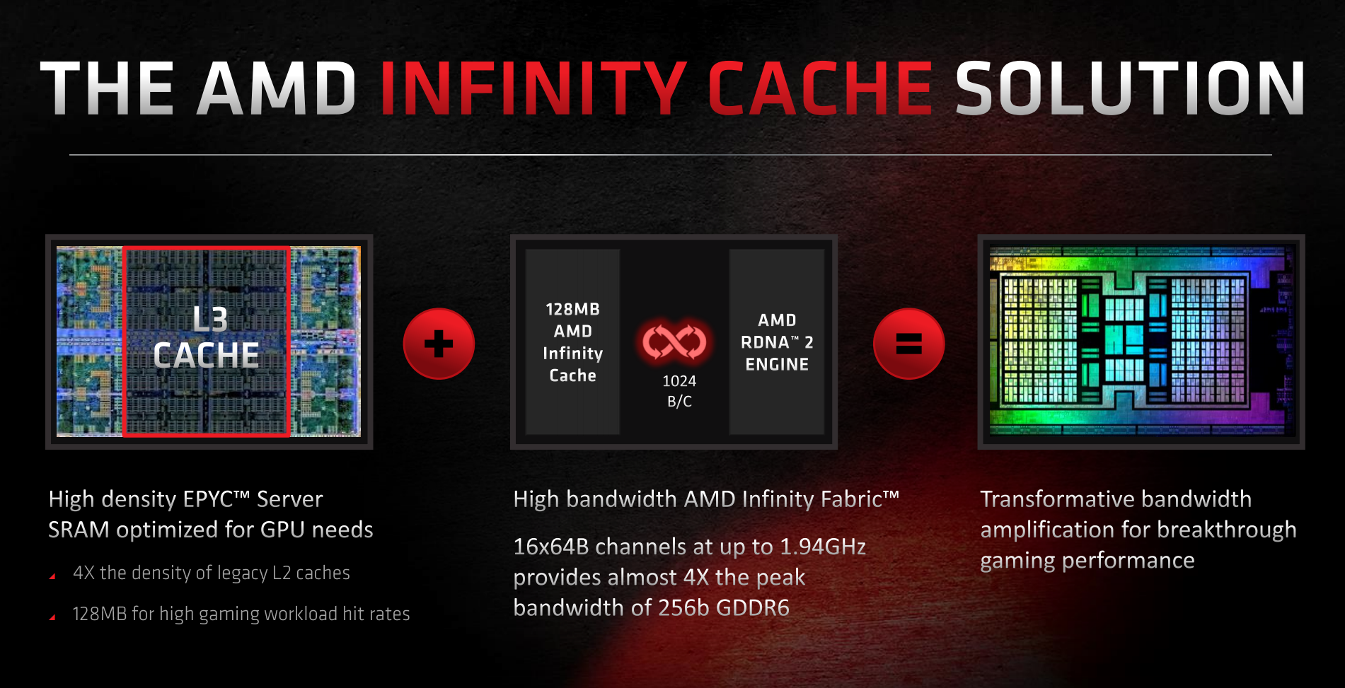
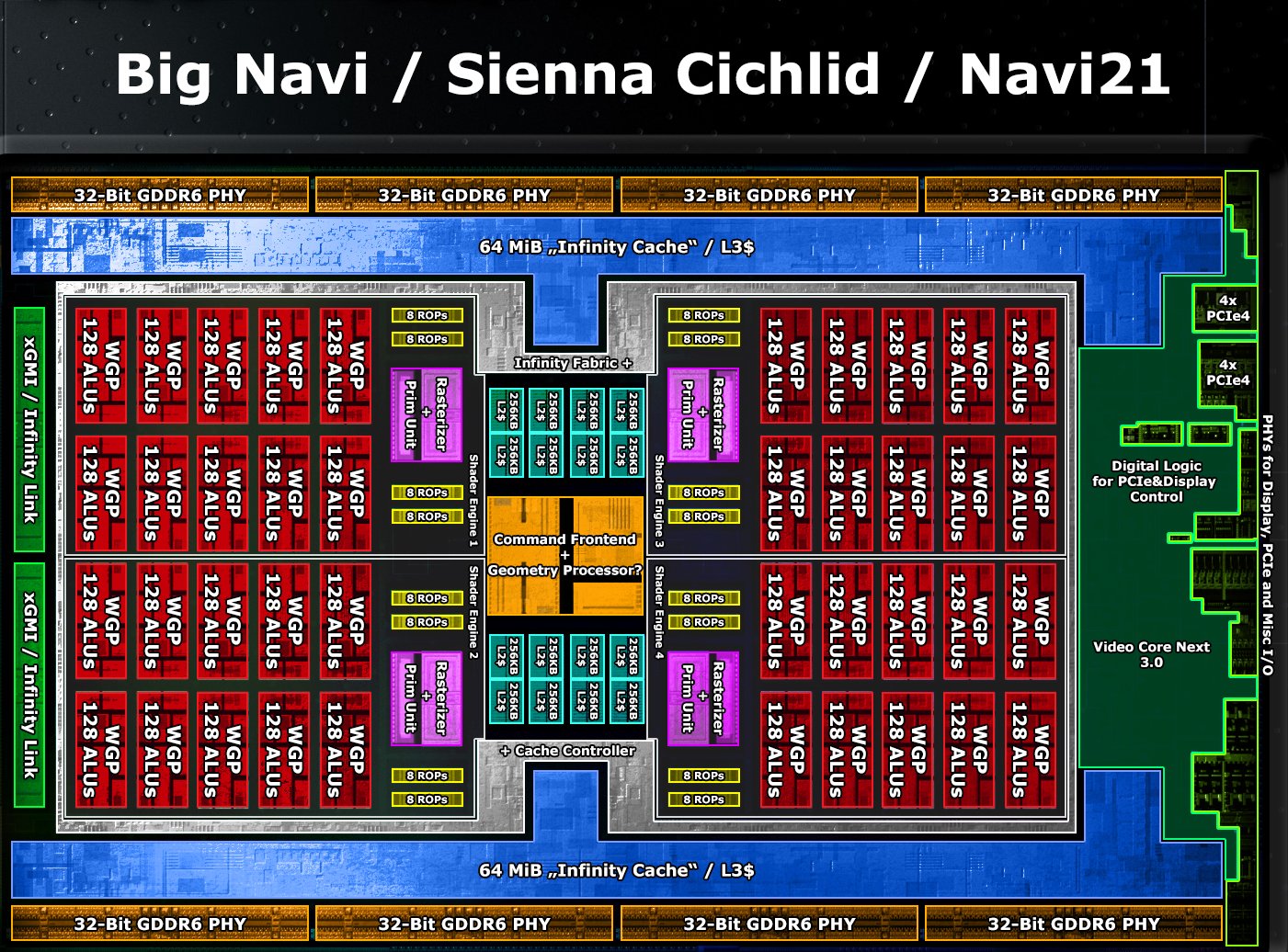
If you look at the graphic
 Loxus
Loxus
posted, the IC, if present, would fit in two likely 8 MB banks per side. I'm trying to visualize a scale from the last image linked here.
I still won't
outright say IC is there, but
IF it's present, there are enough design parallels between PS5's GPU setup and the RDNA 2 GPU references linked to support some possibility of a 16 MB (low end) - 32 MB (upper limit) Infinity Cache. That'd be enough theoretically for a 4K framebuffer (24.8832 MB), tho that's probably not actually enough for a true 4K framebuffer since it seems 128 MB is "just enough" for 4K on PC RDNA 2 GPUs. For smaller framebuffers though, 32 MB would be pretty good, 16 MB less so but we can't rule that out either.
And again, we CAN'T rule out the possibility there's no IC present at all; I'm just saying going off these die shots and graphs that there's some possibility a limited IC capacity implementation is present in PS5, that's all. Ironically if 32 MB that'd make it roughly the same as the eSRAM in the Xbox One (I think AMD took some inspiration from the eSRAM on XBO for going with IC on the RDNA 2 GPUs, at least partially. Maybe that's a kind of ironic, I dunno).

www.gamesindustry.biz
")


") .
.


