You are using an out of date browser. It may not display this or other websites correctly.
You should upgrade or use an alternative browser.
You should upgrade or use an alternative browser.
PS5 Die Shot has been revealed
- Thread starter LivingD3AD
- Start date

thicc_girls_are_teh_best
Member
Good breakdown; I think this was MS's thinking process in all honesty, and as you said, there is nothing inherently bad with this approach. It's just a different one compared to Sony, equally as interesting and useful though, particularly for Microsoft's use-cases.Could it be 4 SE with 1 SA per SE? Perhaps. Doesn't look that way tho. Idk.
If you look at the slide with their GPU layout, it has 2 things labeled shader input. Those would seem to indicate 2 shader engines, idk.
The 2 groups of 28 CUs are also spaced further apart in 2 groups, which also seems clear that its 4 SA but 2 SE.
And btw, none of this is a criticism of the XSX. Just my thoughts and guesses.
Thats not what that poster meant. I don't know or care what that youtuber guy said but Phil Spencer himself has said the XSX SoC was designed with the Azure silicon engineer team as well. That's why Azure engineers did the hot chips presentation. The chip was built for multiple purposes, console chip and xcloud server chip.
Thats why Xbox have said the XSX when used in xcloud servers can run 4 Xbox One games simultaneously from 1 SoC. Because it was built for that as well. Thats why in their recent presentation they discuss the flexibility of the CU design to serve both console & cloud server roles.

"Multiple uses" refers to use in console (XSX) and cloud (xcloud server.)
Xbox Cloud Gaming refers to when used in cloud servers. They only need 24 DCUs, 48 CUs total. Because Xbox One games use 12 CUs each. Each Xbox One has 7 DCUs on chip, 6 active. Thats why they built the XSX GPU to be 4 arrays of 7 DCUs. To be able to run 4 Xbox One games at once from 1 chip. Xbox One games use 5 GB RAM. For 4 games, the server chip would need 20 GB RAM. For the typical setup of 20 GB RAM, one would use either 10x 2 GB RAM chips or 20x 1 GB RAM chips, connected to a 320 bit interface. Thats most likely why the XSX console has the 320 bit bus but split bandwidth setup with 16 GB RAM. They wanted more bandwidth than 448 GB/s, and wanted the 320 bit bus on die for its secondary use in xcloud, but didn't want to spend the extra cash per console to put 20 GB RAM in each XSX. And using faster 16 Gb/s G6 RAM would have also cost more and or increased heat generated inside the console.
Plus, normally, any XSX chip that doesn't yield 52 CUs would end being wasted. But for using in xcloud, they only need 48, so they can actually save extra money and use more of the chips per wafer that they're paying TSMC to make for them. Its a clever way of building 1 chip that can serve 2 roles.
This is why once they determined they had 52 active CUs in the XSX, they just picked the clock speed to achieve 12 TFLOPS which Phil said was their goal all along. They did the same thing with XOneX, where they arrived at 40 active CUs and set the oddly specific clock of 1.172 GHz needed to get exactly 6.0 TFLOPs. And the same thing with XSS. Its a 20 CU GPU, and their goal was 4 TFLOPs, so they set clock to exactly 1.565 GHz to get exactly 4.0 TFLOPs.
I think the major problem with guys like MLID is, they take this type of info and phrase it with a lot of loaded negative, mocking, condescending connotations. I've see the vids he did when responding to this console stuff, there is a tone of dismissiveness and hostility from him when discussing the Series X in relation to PS5, and no that isn't something "only fanboys would say", to take the type of phrasing he'd like to use.
The way he's handling the fallout from the die shot stuff speaks enough to his personality in this regard, but I just wanted to touch on this specific part really quick. Because, again, he's used the highly-probable fact of Series X being designed for dual purposes as an implied/laced insult towards the platform in relation to PlayStation 5 in his console discussions, and coerced some of his guests to go along with it. Someone who wants to be seen as a neutral priority figure in the space of discussing technology leaks, or come off as a professional (when they have literal professionals from certain tech fields as guests from time to time), wouldn't stoop to the depths MLID tends to do in referring to boogeyman fanboys (usually Xbox ones) semi-regularly, or regularly using things like a system being simultaneously designed with a server/cloud purpose as an insult or dismissive perspective on said system.
That's honestly my biggest red flag with him and techtubers with supposed insider connects who engage in similar behavior.
HoofHearted
Member
kyliethicc
Member
Yeah I get that it can used as a negative criticism but I'm not intending that at all. Its just literally a fact of the SoC design that Phil Spencer himself described. The console silicon is designed collaboratively with the Azure cloud engineers. The chip needs to be used in console but also in xcloud servers.Good breakdown; I think this was MS's thinking process in all honesty, and as you said, there is nothing inherently bad with this approach. It's just a different one compared to Sony, equally as interesting and useful though, particularly for Microsoft's use-cases.
I think the major problem with guys like MLID is, they take this type of info and phrase it with a lot of loaded negative, mocking, condescending connotations. I've see the vids he did when responding to this console stuff, there is a tone of dismissiveness and hostility from him when discussing the Series X in relation to PS5, and no that isn't something "only fanboys would say", to take the type of phrasing he'd like to use.
The way he's handling the fallout from the die shot stuff speaks enough to his personality in this regard, but I just wanted to touch on this specific part really quick. Because, again, he's used the highly-probable fact of Series X being designed for dual purposes as an implied/laced insult towards the platform in relation to PlayStation 5 in his console discussions, and coerced some of his guests to go along with it. Someone who wants to be seen as a neutral priority figure in the space of discussing technology leaks, or come off as a professional (when they have literal professionals from certain tech fields as guests from time to time), wouldn't stoop to the depths MLID tends to do in referring to boogeyman fanboys (usually Xbox ones) semi-regularly, or regularly using things like a system being simultaneously designed with a server/cloud purpose as an insult or dismissive perspective on said system.
That's honestly my biggest red flag with him and techtubers with supposed insider connects who engage in similar behavior.
"We need a console chip and a cloud server chip, we only have some many wafers from TSMC, why not design 1 chip that can do both?"
Its perfectly smart business by Microsoft to be efficient with their resources. And once I read those quotes about the dual purpose design, and read their various presentation slides, and now looking at their console design again, its fairly easy to see what their thinking was when building it.
I honestly don't care or know much about any of these tech youtubers. Personally, all I know is that last year, the guy said God of War would get revealed at the 2nd PS5 showcase and be dated for 2021, and that was correct. He has now said Bluepoint is remaking MGS. As a future owner of the PS5 (fucking eventually) I simply hope this is true cause I'd like to play that game. That's all I know or give a shit about in regards to that guy.
Last edited:
Kumomeme
Member
So when are we gonna talk about the games?

thicc_girls_are_teh_best
Member

lol no you didn't!


He added one more piece.
This feels like when Microsoft roasted DarkSydePhil in a tweet. Are
Mind. Blown.
I kid but, ethomaz c'mon, you're trying to say a hardware engineer on the console itself is wrong about the system he helped build. You know you were gonna lose that fight before it even started xD
Yeah I get that it can used as a negative criticism but I'm not intending that at all. Its just literally a fact of the SoC design that Phil Spencer himself described. The console silicon is designed collaboratively with the Azure cloud engineers. The chip needs to be used in console but also in xcloud servers.
"We need a console chip and a cloud server chip, we only have some many wafers from TSMC, why not design 1 chip that can do both?"
Its perfectly smart business by Microsoft to be efficient with their resources. And once I read those quotes about the dual purpose design, and read their various presentation slides, and now looking at their console design again, its fairly easy to see what their thinking was when building it.
I honestly don't care or know much about any of these tech youtubers. Personally, all I know is that last year, the guy said God of War would get revealed at the 2nd PS5 showcase and be dated for 2021, and that was correct. He has now said Bluepoint is remaking MGS. As a future owner of the PS5 (fucking eventually) I simply hope this is true cause I'd like to play that game. That's all I know or give a shit about in regards to that guy.
That is the weird part with MLID; he did get the GoW stuff right...though I'm starting to wonder now if he just scrounged around other forums and subreddits and saw a few randoms mentioning it before bringing it up himself. Still though, at least on something like MGS remake with Bluepoint, I think it's safe to put faith in it because it just kind of makes sense.
Otherwise yeah, Microsoft's choice with dual-purposing their Series X chip was incredibly smart. Maybe the only design decision from them that's still questionable is not going with 20 GB of RAM; if there's any growing pains with the segmented memory approach still being ironed out I'm sure they will eventually be resolved but, all of that could've been avoided with just an extra 4 GB per system.
They might not have even needed 320-bit bus for that (though that's just a quick thought; I've been reading
But, given the scale of the companies making these things, I'm pretty sure they considered this at some point and something either with the memory setup or costs (or both) didn't meet their requirements. Interesting thought experiment tho.
Last edited:
SenjutsuSage
Banned
Good breakdown; I think this was MS's thinking process in all honesty, and as you said, there is nothing inherently bad with this approach. It's just a different one compared to Sony, equally as interesting and useful though, particularly for Microsoft's use-cases.
I think the major problem with guys like MLID is, they take this type of info and phrase it with a lot of loaded negative, mocking, condescending connotations. I've see the vids he did when responding to this console stuff, there is a tone of dismissiveness and hostility from him when discussing the Series X in relation to PS5, and no that isn't something "only fanboys would say", to take the type of phrasing he'd like to use.
The way he's handling the fallout from the die shot stuff speaks enough to his personality in this regard, but I just wanted to touch on this specific part really quick. Because, again, he's used the highly-probable fact of Series X being designed for dual purposes as an implied/laced insult towards the platform in relation to PlayStation 5 in his console discussions, and coerced some of his guests to go along with it. Someone who wants to be seen as a neutral priority figure in the space of discussing technology leaks, or come off as a professional (when they have literal professionals from certain tech fields as guests from time to time), wouldn't stoop to the depths MLID tends to do in referring to boogeyman fanboys (usually Xbox ones) semi-regularly, or regularly using things like a system being simultaneously designed with a server/cloud purpose as an insult or dismissive perspective on said system.
That's honestly my biggest red flag with him and techtubers with supposed insider connects who engage in similar behavior.
Nailed it. Series X can both get 100% of the power as labeled on the paper specs for gamers while at the same being an awesome cloud server chip for game streaming. Simply because it has dual use doesn't automatically cripple the SoC in a console where its primary function will be as a games console.
The reason I don't trust Moores Law, and honestly nobody who is looking for credible information on anything pertaining to Playstation and Xbox should, is exactly due to that hostility he showed. It seemed more personal, targeted smear campaign. I may disagree with RGT, and feel he spreads some nonsense, too, but the way he does what he does generally makes him come off a whole lot more respectful about the things he discusses, even when he's hyping PS5. That hostility MLID showed isn't present, and that makes all the difference in your willingness to give the person a chance.
thicc_girls_are_teh_best
Member
Yeah, pretty much. Guys like RGT have a preference I'm sure, but they don't let that bleed into a bias against a different brand. He's gone with a few clickbait titles himself but in terms of the actual delivery he usually tries to not delve into dogging down a given platform. In that way they keep it generally professional.Nailed it. Series X can both get 100% of the power as labeled on the paper specs for gamers while at the same being an awesome cloud server chip for game streaming. Simply because it has dual use doesn't automatically cripple the SoC in a console where its primary function will be as a games console.
The reason I don't trust Moores Law, and honestly nobody who is looking for credible information on anything pertaining to Playstation and Xbox should, is exactly due to that hostility he showed. It seemed more personal, targeted smear campaign. I may disagree with RGT, and feel he spreads some nonsense, too, but the way he does what he does generally makes him come off a whole lot more respectful about the things he discusses, even when he's hyping PS5. That hostility MLID showed isn't present, and that makes all the difference in your willingness to give the person a chance.
Moore's Law, as well, in his case it's obvious he has a preference but the difference is several times he's used that as a negative bias towards a different brand, in this case Xbox console discussion, and in some ways that extends to Gamepass as well which is frustrating because I think he brings up good points overall but the hostility and pessimism he seems to give off when discussing a lot of things related to Xbox and Gamepass is not the best of taste. Like on Twitter he singled out literally one Xbox fanboy's comment as if it were a legion of Xbox fans dogging him over the die shot and x-rays for PS5 SoC. I'm pretty sure a lot of Xbox fans would look at that user and laugh at them too for being a blatant fanboy, I don't see why MLID highlighted such a tweet as if it's a large swath of Xbox fans behaving that way on Twitter though.
Again, his gaming preferences aren't an issue at all. We all having preferences when it comes to gaming, it's normal. But letting those develop into a negative bias towards things outside of those preferences IS a problem, and I think MLID is guilty of that when it comes to Xbox. You can tell at times by the way he talks about it when framed against PS5. If it was the inverse, I'd have just as much an issue and there's actually some Xbox-centric Youtubers who do that whom I take issue with as well, but those would be bridges to cross if they ever had something blow up in their face like the rumors attached to MLID have (and if they handled the fallout as poorly as he has with this one).
Last edited:
So when are we gonna talk about the games?
This is the worst start of any generation, ever. Consoles are still not in stock, no compelling games (particularly on MS console(s)) and endless bickering over APU differences, supposed console issues. I have been around video games (formats/platforms) since early 80's, and have never seen so much negativity and sometimes downright hostility.
Last edited:
SenjutsuSage
Banned
Okay, so the upgraded Compute Units inside RDNA 2 are where Series X gets Sampler Feedback/Texture Space Shading support from. And then of course we know Microsoft added on additional hardware to further improve texture streaming, which they've mentioned quite a few times now. And of course Mesh Shaders is clearly in the Geometry Engine.

The Series X GPU's L2 cache is also bigger than the L2 inside RX 6800 XT. On PC RDNA 2, the L2 cache is 4MB, on Series X it's 5MB.


What I still can't figure out is where the hell is Series X getting 76MB of SRAM from that was confirmed to Digital Foundry? Can't find it anywhere, but then there are security stuff inside we know very little about. Plus I'm guessing there must be some on the audio and other hardware too. Who knows honestly lol. Off to bed.
The Series X GPU's L2 cache is also bigger than the L2 inside RX 6800 XT. On PC RDNA 2, the L2 cache is 4MB, on Series X it's 5MB.
What I still can't figure out is where the hell is Series X getting 76MB of SRAM from that was confirmed to Digital Foundry? Can't find it anywhere, but then there are security stuff inside we know very little about. Plus I'm guessing there must be some on the audio and other hardware too. Who knows honestly lol. Off to bed.
Red_Driver85
Member
And of course Mesh Shaders is clearly in the Geometry Engine.

93xfan
Banned
You came to a tech thread to discuss gameplay? Do you also come to music threads and ask why no one is discussing the story?So when are we gonna talk about the games?
You came to a tech thread to discuss gameplay? Do you also come to music threads and ask why no one is discussing the story?
I think you missing the point. IMO. It was a rhetorical question. Sorely needed, in a thread full of endless drivel by dilettantes mostly.
Last edited:
SenjutsuSage
Banned
Way to follow the convo.
Someone said MS paid for the "Big navi" design to get more CUs.
Which of course is total rubbish.
RDNA 2 is 10 CUs per shader engine (as per the PS5 regardless of any that are disabled)
As I said MS had AMD fit more CU's in the shader array, they did not buy a "big navi" design.
PS5 and Series X both have 2 shader engines.
Series X is only "scarily" close to the 6800 if you add some fanboyism and squint your eyes.
"The RX 6800 is further cut down by enabling 60 out of 80 CUs. It's unclear if a full Shader Engine or 10 random Dual CUs have been disabled to accomplish this." (this is from tech powerup's write up of the 6800 series)
So it has 3 or 4 shader engines (most likely 4 as requiring 3 fully functional shader engines probably misses the point of disabling some for yeilds anyway) enabled with 10 DCUs as per PS5 and all other RDNA2 cards with 10 CUs disabled across the board.
There is no 14 CU shader engine design for RDNA 2 besides what MS have asked for.
I checked some sites, RX 6800 indeed has 3 shader engines apparently, which is so weird, but I won't attempt to understand it lol.
None of that changes how super close Series X's GPU still is to an RX 6800. it's literally only missing 2 more dual compute units to be a 60 CU part. TWO. If not for obvious cost cutting and power reasons, that 3rd shader engine would be there, and with it would come RX 6800's 32 additional ROPs. Then from there you have yourself a very similar shader engine layout as RX 6800.
I think this only makes my argument stronger. Microsoft could be said to have taken a 96 ROPs 3, Shader Engine and 60 Compute Unit design and had AMD cut it down to a 64 ROPs, 2 Shader Engine and 56 Compute Unit design
So to me evidence is pretty weak that Microsoft did not in fact still start out with a "big navi" design only to have AMD fit it to their needs. I really don't think the 10 Dual CU shader engine design is a good bit of proof that couldn't have been the case because these things - console and PC designs - were obviously developed concurrently.
Again, 2 dual CUs short of having as many as RX 6800. One of Microsoft's very own Xbox architects pretty much made clear their base was RDNA 2 from the jump.
I also don't buy that the 10 shader engine design is the best one for utilization purposes whoever made that claim, not sure if you did. The architecture from the start is built to scale by nature. Developers will get better at targeting these strengths, and a seemingly more beefier shader array/engine design is something Microsoft will make certain ends up being to their benefit. They know best what they have in mind for the system. It was done for a very good reason.
All things considered, you are in the end correct about one thing, the Series X does indeed possess the only 14 Dual Compute Compute Unit Shader Engine design for RDNA 2 GPUs in existence. I actually find that fact pretty fucking exciting.
Popup
Member
I just wish we would stick to trying to better uncover, speculate about and try to understand the more bespoke features and design choices of this rather than arguing over semantics.
it all starts sounding a bit pointless if we are talking about C3PO and everyone is like:-

it all starts sounding a bit pointless if we are talking about C3PO and everyone is like:-
Last edited:
longdi
Banned
This feels like when Microsoft roasted DarkSydePhil in a tweet. Areethomaz and DarkSydePhil the same person after all!?
Mind. Blown.
I kid but, ethomaz c'mon, you're trying to say a hardware engineer on the console itself is wrong about the system he helped build. You know you were gonna lose that fight before it even started xD
That is the weird part with MLID; he did get the GoW stuff right...though I'm starting to wonder now if he just scrounged around other forums and subreddits and saw a few randoms mentioning it before bringing it up himself. Still though, at least on something like MGS remake with Bluepoint, I think it's safe to put faith in it because it just kind of makes sense.
Otherwise yeah, Microsoft's choice with dual-purposing their Series X chip was incredibly smart. Maybe the only design decision from them that's still questionable is not going with 20 GB of RAM; if there's any growing pains with the segmented memory approach still being ironed out I'm sure they will eventually be resolved but, all of that could've been avoided with just an extra 4 GB per system.
They might not have even needed 320-bit bus for that (though that's just a quick thought; I've been readingLocuza 's posts and from that and a few other posts including yours and
Loxus 's there might be design implications to the GPU setup for Azure cloud intent to go with 320-bit, for example for capacity purposes in Azure racks); 288-bit bus with 9x 16 Gbps chips for 576 GB/s. Both higher peak bandwidth and all unified, maybe only slightly more costs vs. the 10 chip setup they've gone with.
But, given the scale of the companies making these things, I'm pretty sure they considered this at some point and something either with the memory setup or costs (or both) didn't meet their requirements. Interesting thought experiment tho.
MILD is full of shit. RGT too. They just go around forums and reddits, especially Chinese forums which have tons more noise since they are closer to the manufacturers.
When you throw tons of rumors and see which sticks. GOW is a simple guess, like GT7 or FF15.
How many rumors and dozens of videos they made, have anything substantial? RGT probably got to contact someone working at Amd marketing or what, and he got 2 things right. As for the rest of his videos, just nothing more than forums rumors. Some even got from GAF.
Hi RGT!
93xfan
Banned
It's like coming in and saying "who cares about the tech? it's all about the games." Everyone here cares about the tech to some degree.I think you missing the point. IMO. It was a rhetorical question. Sorely needed, in a thread full of endless drivel by dilettantes mostly.
Would a thread about which has the better exclusives be served well by someone jumping in and saying "but the teraflops"?
Tech threads are about tech. Anyone wishing to talk about exclusives can find one of many threads talking about that.
assurdum
Banned
Cerny said really very few and basic things about GE if we want to be honest.all we have to know about ps5 geometry engine was on road to ps5 :
what did Cerny said about it ?
* this is where people loose the thread and think it's about geometry engine when it's about primitive shader simple usage (or simple programmatic control example if you prefer). this is also the point where youtuber can make click bait speculation video. those speculation are laughtable to me because they talk about fixed function advantage when the feature is about overriding/replacing/not using them.
What describe here is also in line with amd and nvidia implementations and dx12u specs of primitive/mesh shader.
Amd ones struggling hard on vega/rdna1 and now working on rdna2
is that the result of a successful collaboration seen in a gpu launched roughly at the same as ps5 ? it seems like it.
Will one perform better ? ps5 has GMM and higher clock advantage and xsx has more units so it will depends
Also unlike what i though this trend to replace fixed hw function by shader workload is also true and give better result for vrs especially in deferred engine

Black_Stride
do not tempt fate do not contrain Wonder Woman's thighs do not do not
Please note: While we know that MS has ML capabilities, we do not know what Sony has. Looking at comments from various parties the jury is still out on that one. Locusa above has good arguments why ML probably is not there. Leviathangamer has good arguments for why it most likely is there.
Personally, I have no idea")
This probably the smartest thing anyone has said in this thread.
I have no idea how this thread is 38 pages......is everyone on GAF an Engineer
MILD is full of shit. RGT too. They just go around forums and reddits, especially Chinese forums which have tons more noise since they are closer to the manufacturers.
When you throw tons of rumors and see which sticks. GOW is a simple guess, like GT7 or FF15.
How many rumors and dozens of videos they made, have anything substantial? RGT probably got to contact someone working at Amd marketing or what, and he got 2 things right. As for the rest of his videos, just nothing more than forums rumors. Some even got from GAF.
Hi RGT!
I dont know why people hang on their videos like scripture.
They basically regurgitate rumors they found on forums and yes sometimes said rumors come true.
But even a broken clock is right twice.
So people who quote them make me laugh might as well just quote any random NeoGAF poster you like whose uncle works at Nintendo.
RGT and MLID are both trash and shouldnt be used as sources for anything, if GAF still had banned sources those two would need to be towards the top.
Yes, but totally forget the power target. Xbox has around 225w (I guess it is around 250w if cpu and gpu are maxed out in later titles) for the whole console. The 6800 can go beyond that all the time, just for the gpu.The card runs way higher than that lol


Same for RX 6800 XT.

That was s why the 6800 can operate beyond the 1815mhz and promised. But you might just get a card that really only reaches the promised clocks and not much more.
Physiognomonics
Member
This is about efficiency. you need what's inside the shader array to correctly use the CUs and for rasterization, polygons creations, alpha effects etc. Why bother with several shader array at all? Why not using only one shader array for 100CUs? Because you need CUs for compute and the shader array stuff for the rest (and properly use compute). It's a balance and all big RDNA GPUs are balanced with 5 DCUs by shader array, even the biggest ones. There is a good reason for that.Oh god, that nonsense from Moore's law again. The console has access to all 12 TFLOPS for gaming. There isn't any performance dedicated solely to cloud computing.
But the comparisons are telling us this story whether you want it or not. XSX is not performing like a 12TF RDNA GPU, it's actually performing under PS5 so we could say currently on average XSX is performing like a 9TF GPU during gameplay.
Riky
$MSFT
This is about efficiency. you need what's inside the shader array to correctly use the CUs and for rasterization, polygons creations, alpha effects etc. Why bother with several shader array at all? Why not using only one shader array for 100CUs? Because you need CUs for compute and the shader array stuff for the rest (and properly use compute). It's a balance and all big RDNA GPUs are balanced with 5 DCUs by shader array, even the biggest ones. There is a good reason for that.
But the comparisons are telling us this story whether you want it or not. XSX is not performing like a 12TF RDNA GPU, it's actually performing under PS5 so we could say currently on average XSX is performing like a 9TF GPU during gameplay.
Hitman 3 says otherwise, 44% resolution advantage and higher settings across the entire game, not just in small parts or variable, but constant.
Last edited:
Panajev2001a
GAF's Pleasant Genius
For Control, but it can apply to more games than that. Keep championing that one game in those spots and ignore everything else.Hitman 3 says otherwise, 44% resolution advantage and higher settings across the entire game, not just in small parts or variable, but constant.

Panajev2001a
GAF's Pleasant Genius
Also, having a lot of CU's per array and the same array cache does not mean you get no speed up at all thanks to the additional CU's, but that you open up to cases where we have less speed up than expected.This is about efficiency. you need what's inside the shader array to correctly use the CUs and for rasterization, polygons creations, alpha effects etc. Why bother with several shader array at all? Why not using only one shader array for 100CUs? Because you need CUs for compute and the shader array stuff for the rest (and properly use compute). It's a balance and all big RDNA GPUs are balanced with 5 DCUs by shader array, even the biggest ones. There is a good reason for that.
But the comparisons are telling us this story whether you want it or not. XSX is not performing like a 12TF RDNA GPU, it's actually performing under PS5 so we could say currently on average XSX is performing like a 9TF GPU during gameplay.
Riky
$MSFT
For Control, but it can apply to more games than that. Keep championing that one game in those spots and ignore everything else.
If that was true then Series X would have won all the original comparisons early on, the likes of the Ubisoft games are all last gen engines.
Like DF said, only have 36 compute units and a level memory bandwidth situation like PS4 Pro actually makes the opposite true.
DJ12
Member
Of course you don't, I would never expect an xbox fanboy to think that an actual company that designs GPUs for their livelihood, would have a better idea of how to make a GPU than MS.I also don't buy that the 10 shader engine design is the best one for utilization purposes whoever made that claim, not sure if you did. The architecture from the start is built to scale by nature. Developers will get better at targeting these strengths, and a seemingly more beefier shader array/engine design is something Microsoft will make certain ends up being to their benefit. They know best what they have in mind for the system. It was done for a very good reason.
All things considered, you are in the end correct about one thing, the Series X does indeed possess the only 14 Dual Compute Compute Unit Shader Engine design for RDNA 2 GPUs in existence. I actually find that fact pretty fucking exciting.
You can take it as fact that 10 is the sweet spot, else AMD would have more CUs in their own cards arrays. I'm sorry you are trying to spin the arrays in the Series S|X console being unbalanced as a good thing, but I guess this is your level of fanboying so no worries.
Better would've been to have 3 balanced shader engines with 1 DCU disabled on each one, I guess that would've added far more to the die size though than MS were willing to risk, probably a wise choice considering how relatively low the yields are reported to be for the Series X SOC anyway.
Last edited:
geordiemp
Member
I checked some sites, RX 6800 indeed has 3 shader engines apparently, which is so weird, but I won't attempt to understand it lol.
None of that changes how super close Series X's GPU still is to an RX 6800. it's literally only missing 2 more dual compute units to be a 60 CU part. TWO. If not for obvious cost cutting and power reasons, that 3rd shader engine would be there, and with it would come RX 6800's 32 additional ROPs. Then from there you have yourself a very similar shader engine layout as RX 6800.
I think this only makes my argument stronger. Microsoft could be said to have taken a 96 ROPs 3, Shader Engine and 60 Compute Unit design and had AMD cut it down to a 64 ROPs, 2 Shader Engine and 56 Compute Unit design
So to me evidence is pretty weak that Microsoft did not in fact still start out with a "big navi" design only to have AMD fit it to their needs. I really don't think the 10 Dual CU shader engine design is a good bit of proof that couldn't have been the case because these things - console and PC designs - were obviously developed concurrently.
Again, 2 dual CUs short of having as many as RX 6800. One of Microsoft's very own Xbox architects pretty much made clear their base was RDNA 2 from the jump.
I also don't buy that the 10 shader engine design is the best one for utilization purposes whoever made that claim, not sure if you did. The architecture from the start is built to scale by nature. Developers will get better at targeting these strengths, and a seemingly more beefier shader array/engine design is something Microsoft will make certain ends up being to their benefit. They know best what they have in mind for the system. It was done for a very good reason.
All things considered, you are in the end correct about one thing, the Series X does indeed possess the only 14 Dual Compute Compute Unit Shader Engine design for RDNA 2 GPUs in existence. I actually find that fact pretty fucking exciting.
Your totally missing the point of a shader engine, think of it as a stand alone thing, so 6800 has three of them that is really parrallel working. Psr5 and XSX and 6700 will have 2 and think of that as a gaming power bracket.
Each shader array has its own resource, like a castle that has food stores, armoury, so many beds to sleep in. You cant just chuck more and more soldiers into 1 castle and start to find a lack of resourse depending on what job soldier is trying to do.
A shader engine shares lots of things, parameter caches, local data stores and thats why you cant keep adding CU forever as efficiency goes down for gaming (not for compute). Thats why Vega is still used for compute and there are more CU in servers per shader engine. How moch of an effect depends on the workload.
Some workloads do favour more CU in shadfer arrays, some do not.
Last edited:
The Hamburglar
Banned
Honestly riky how many times have you said this exact same sentence across all the different threads? Probably 44 times by now.Hitman 3 says otherwise, 44% resolution advantage and higher settings across the entire game, not just in small parts or variable, but constant.
MasterCornholio
Member
Your totally missing the point of a shader engine, think of it as a stand alone thing, so 6800 has three of them that is really parrallel working. Psr5 and XSX and 6700 will have 2 and think of that as a gaming power bracket.
Each shader array has its own resource, like a castle that has food stores, armoury, so many beds to sleep in. You cant just chuck more and more soldiers into 1 castle and start to find a lack of resourse depending on what job soldier is trying to do.
A shader engine shares lots of things, parameter caches, local data stores and thats why you cant keep adding CU forever as efficiency goes down for gaming (not for compute). Thats why Vega is still used for compute and there are more CU in servers per shader engine. How moch of an effect depends on the workload.
Some workloads do favour more CU in shadfer arrays, some do not.
Welcome back.
DForce
NaughtyDog Defense Force
If that was true then Series X would have won all the original comparisons early on, the likes of the Ubisoft games are all last gen engines.
Like DF said, only have 36 compute units and a level memory bandwidth situation like PS4 Pro actually makes the opposite true.
He said SOME last gen engines. I don't know why you're pretending to know more than him about how engines work.
Locuza
Member
It's 76MiB of SRAM across the chip and many structures use SRAM cells.
What I still can't figure out is where the hell is Series X getting 76MB of SRAM from that was confirmed to Digital Foundry? Can't find it anywhere, but then there are security stuff inside we know very little about. Plus I'm guessing there must be some on the audio and other hardware too. Who knows honestly lol. Off to bed.
For example:
CPU:
8x 32 KiB L1 I$ = 256KiB
8x 32 KiB L1 D$ = 256 KiB
8x 512 KiB L2$ = 4 MiB
2x 4MiB L3$ = 8 MiB
The micro-op cache uses SRAM cells, the same amount as the L1I$, you might also count that as 256KiB total.
Branch Target Buffers are even larger than that, then you have Translation Lookaside Buffers, all use SRAM cells and could be added to that number.
So at the very least you have 12.5MiB for the CPU alone.
GPU:
Each WGP has following resources:
4x SIMD32 Units which have each 128KiB of Registers using SRAM = 512 KiB just for Registers per WGP
1x 128 KiB Local Data Share for all Units
1x 32 KiB Instruction Cache
1x 16 KiB Scalar Data Cache
4 x 10 KiB for the Scalar Register File = 40 KiB
2x 16 KiB L0/Tex$ = 32 KiB
Texture Units have extra Buffers and this and that has extra buffers, just counting the stuff above accumalates to 760 KiB per WGP.
The Xbox Series X has 28 WGPs so that's 21.28MiB of SRAM.
Then we have 4x L1$ Cache each being 128KiB in size = 512 KiB total.
1x 5 MiB L2$
GCN2 had 16 KiB Color Cache for each Render Backend + 4 KiB Depth Cache.
If that's still the same then we are looking at 16 x 20 KiB = 320 KiB. (That's an old Copy&Paste section, the new Render Backend has a different configuration but it doesn't change the endresults much)
The Parameter Cache was 1 MiB large on the Xbox One X, Vega doubled that if I remember correctly.
So for the GPU alone I have currently 29.11MiB
Together with the CPU ~41.6MiB
Video encoder/decoder are using a lot of SRAM for their workset, you have a strong Audio DSP system which also uses SRAM, the decompression blocks too.
Command Processor is adding about 48 KiB or more, 1x GDS is 64 KiB large, again several SRAM buffers are not counted on the WGP/CU side, Memory Controller uses SRAM, Display Controllers use SRAM, like everything uses Kibibytes or Mebibytes of SRAM.
To get a better feeling one can look at Trinity:

All the small white lines/blocks inside a tile are SRAM, i's nearly everywhere across the chip.
With the stuff which is easy to count we are already at >41.6 MiB, not too far off the 76 MiB for the whole SoC.
I checked some sites, RX 6800 indeed has 3 shader engines apparently, which is so weird, but I won't attempt to understand it lol.
None of that changes how super close Series X's GPU still is to an RX 6800. it's literally only missing 2 more dual compute units to be a 60 CU part. TWO. If not for obvious cost cutting and power reasons, that 3rd shader engine would be there, and with it would come RX 6800's 32 additional ROPs. Then from there you have yourself a very similar shader engine layout as RX 6800.
I think this only makes my argument stronger. Microsoft could be said to have taken a 96 ROPs 3, Shader Engine and 60 Compute Unit design and had AMD cut it down to a 64 ROPs, 2 Shader Engine and 56 Compute Unit design
So to me evidence is pretty weak that Microsoft did not in fact still start out with a "big navi" design only to have AMD fit it to their needs. I really don't think the 10 Dual CU shader engine design is a good bit of proof that couldn't have been the case because these things - console and PC designs - were obviously developed concurrently.
Again, 2 dual CUs short of having as many as RX 6800. One of Microsoft's very own Xbox architects pretty much made clear their base was RDNA 2 from the jump.
I also don't buy that the 10 shader engine design is the best one for utilization purposes whoever made that claim, not sure if you did. The architecture from the start is built to scale by nature. Developers will get better at targeting these strengths, and a seemingly more beefier shader array/engine design is something Microsoft will make certain ends up being to their benefit. They know best what they have in mind for the system. It was done for a very good reason.
All things considered, you are in the end correct about one thing, the Series X does indeed possess the only 14 Dual Compute Compute Unit Shader Engine design for RDNA 2 GPUs in existence. I actually find that fact pretty fucking exciting.

It's just that 1/4 of the chip is fully disabled.
6800/6800XT/6900XT are all SKUs based on the Navi21 chip which has 4 Shader Engines and 128 Color ROPs.
The Xbox Series X uses a unique GPU design with a different hardware configuration:
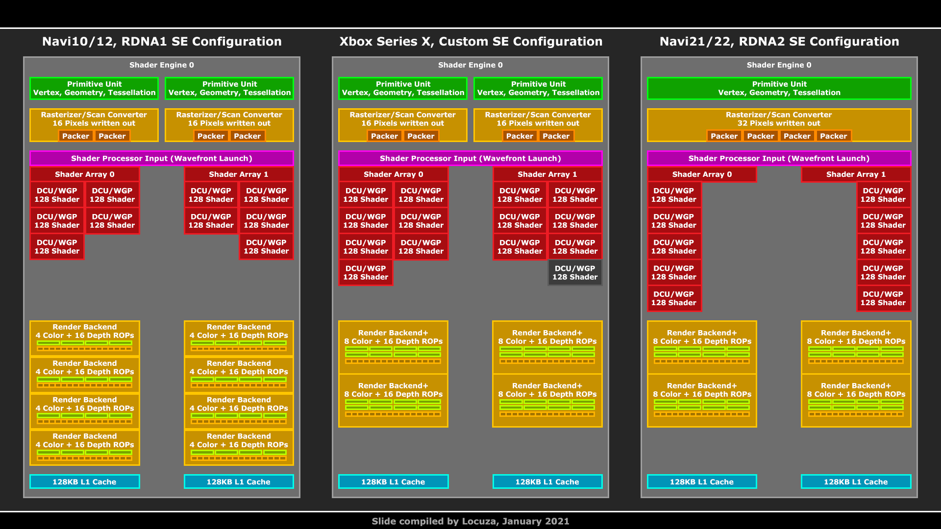
And a different IP set:

It's not directly based/connected to Navi21/the 6800.
And on the die shot the Xbox Series X has physically only 2 Shader Engines, 56 Compute Units and it doesn't have 96 Color ROPs (that would be a massive area waste, having 1/3 of the units disabled).
Last edited:
assurdum
Banned
Probably until the next couple of games which fit her narrative.Honestly riky how many times have you said this exact same sentence across all the different threads? Probably 44 times by now.
PaintTinJr
Gold Member
Surely if the Zen2 CPUs in the PS5 and XsX are a match on Caches then your CPU numbers are massively short AFAIK.It's 76MiB of SRAM across the chip and many structures use SRAM cells.
For example:
CPU:
8x 32 KiB L1 I$ = 256KiB
8x 32 KiB L1 D$ = 256 KiB
8x 512 KiB L2$ = 4 MiB
2x 4MiB L3$ = 8 MiB
The micro-op cache uses SRAM cells, the same amount as the L1I$, you might also count that as 256KiB total.
Branch Target Buffers are even larger than that, then you have Translation Lookaside Buffers, all use SRAM cells and could be added to that number.
So at the very least you have 12.5MiB for the CPU alone.
GPU:
Each WGP has following resources:
4x SIMD32 Units which have each 128KiB of Registers using SRAM = 512 KiB just for Registers per WGP
1x 128 KiB Local Data Share for all Units
1x 32 KiB Instruction Cache
1x 16 KiB Scalar Data Cache
4 x 10 KiB for the Scalar Register File = 40 KiB
2x 16 KiB L0/Tex$ = 32 KiB
Texture Units have extra Buffers and this and that has extra buffers, just counting the stuff above accumalates to 760 KiB per WGP.
The Xbox Series X has 28 WGPs so that's 21.28MiB of SRAM.
Then we have 4x L1$ Cache each being 128KiB in size = 512 KiB total.
1x 5 MiB L2$
GCN2 had 16 KiB Color Cache for each Render Backend + 4 KiB Depth Cache.
If that's still the same then we are looking at 16 x 20 KiB = 320 KiB. (That's an old Copy&Paste section, the new Render Backend has a different configuration but it doesn't change the endresults much)
The Parameter Cache was 1 MiB large on the Xbox One X, Vega doubled that if I remember correctly.
So for the GPU alone I have currently 29.11MiB
Together with the CPU ~41.6MiB
Video encoder/decoder are using a lot of SRAM for their workset, you have a strong Audio DSP system which also uses SRAM, the decompression blocks too.
Command Processor is adding about 48 KiB or more, 1x GDS is 64 KiB large, again several SRAM buffers are not counted on the WGP/CU side, Memory Controller uses SRAM, Display Controllers use SRAM, like everything uses Kibibytes or Mebibytes of SRAM.
To get a better feeling one can look at Trinity:
All the small white lines/blocks inside a tile are SRAM, i's nearly everywhere across the chip.
With the stuff which is easy to count we are already at >41.6 MiB, not too far off the 76 MiB for the whole SoC.
It's just that 1/4 of the chip is fully disabled.
6800/6800XT/6900XT are all SKUs based on the Navi21 chip which has 4 Shader Engines and 128 Color ROPs.
The Xbox Series X uses a unique GPU design with a different hardware configuration:
And a different IP set:
It's not directly based/connected to Navi21/the 6800.
And on the die shot the Xbox Series X has physically only 2 Shader Engines, 56 Compute Units and it doesn't have 96 Color ROPs (that would be a massive area waste, having 1/3 of the units disabled).
The PS5 dies shot shows 16MB of L3 cache, 4MB of L2 cache and 512KB of L1 cache if I'm not mistaken, which would give 20.5MB just for the CPU, then add in your 29.11 for the GPU - you calculated, I didn't verify -, we'd be looking at another 24MB for something like a SSD cache on the board - because the SSD's in the XsX are sold cacheless IIRC- and/or network card cache, and/or a secondary ARM chip for background standby stuff.
Last edited:
Red_Driver85
Member
What? It's 8.The PS5 dies shot shows 16MB of L3 cache
In consoles the ideal approach is that architects take the available technologies and customize them, taking what they think it's relevant for their vision to make their own product.
This is why AMD has found success in this business, because they are willing to make actually customized silicon unlike nVidia that doesn't want to be distracted, they just want to sell their chips as they are and make money out of it (they simply sold an old Tegra chip to Nintendo for example).
This thread is basically 40 pages of people guessing what blocks can be classifed as RDNA1, RDNA2 and what feature list they check for console war reasons but this is kinda pointless because there is no global architectural vision into all this while it's this vision that pushed architects to make certain choices in first place.
Isn't the conclusion made here that both are using blocks that seem to be taken from different generations looking just at the layout and size of them? So they're both ''customized''?
If we take the claim that the GPU in XSX is 100% RDNA2 as true it means that this approach of looking at the blocks is wrong somehow but that applies to both at this point.
Most importantly the actual performance of these boxes is already under everyone's nose, this kind of discussion would have been more interesting one year ago.
Ray tracing is already being used in games (and we have ralready seen the kind of performance limitations it brings on both), the much talked VRS is already being used in hardware or software, the performance/watt improvements of RDNA2 are instrinsic of the architecture itself and for example in PS5's case they have allowed for really high clockspeeds, same for the better IPC of the new CPUs.
In the future I guess that mesh shaders and geometry engine will be used and will help both, the faster I/O pipeline will be fully used. It will also be interesting to see what AMD is doing with their DLSS alternative that btw doesn't seem to be machine learning based.
Last edited:
PaintTinJr
Gold Member
I must be doing something wrong, because looking at the three abstracted views - rotating and mirroring the bottom left CPU view at maximum description - across the whole CPU chip, and counting the 8 cores, I'm getting 2MB of L3 per core.What? It's 8.
/I'm now confused what I'm looking at
Last edited:
Surely if the Zen2 CPUs in the PS5 and XsX are a match on Caches then your CPU numbers are massively short AFAIK.
The PS5 dies shot shows 16MB of L3 cache, 4MB of L2 cache and 512KB of L1 cache if I'm not mistaken, which would give 20.5MB just for the CPU, then add in your 29.11 for the GPU - you calculated, I didn't verify -, we'd be looking at another 24MB for something like a SSD cache on the board - because the SSD's in the XsX are sold cacheless IIRC- and/or network card cache, and/or a secondary ARM chip for background standby stuff.
I think Paint is right. Look, I'm extremely out of my element, but the die shot goes into detail for sections. You apply the details to the rest of the shot for the other section it fits.What? It's 8.
This, AFAIK, is right. It didnt make sense until I started looking at the shots more. Reading, looking more, posting less.I must be doing something wrong, because looking at the three abstracted views - rotating and mirroring the bottom left CPU view at maximum description - across the whole CPU chip, and counting the 8 cores, I'm getting 2MB of L3 per core.
/I'm now confused what I'm looking at
This is a major learning experience for me.
Last edited:
Locuza
Member
Surely if the Zen2 CPUs in the PS5 and XsX are a match on Caches then your CPU numbers are massively short AFAIK.
The PS5 dies shot shows 16MB of L3 cache, 4MB of L2 cache and 512KB of L1 cache if I'm not mistaken, which would give 20.5MB just for the CPU, then add in your 29.11 for the GPU - you calculated, I didn't verify -, we'd be looking at another 24MB for something like a SSD cache on the board - because the SSD's in the XsX are sold cacheless IIRC- and/or network card cache, and/or a secondary ARM chip for background standby stuff.
https://pbs.twimg.com/media/EuN_KU0XIAMX6yH?format=jpg&name=4096x4096I must be doing something wrong, because looking at the three abstracted views - rotating and mirroring the bottom left CPU view at maximum description - across the whole CPU chip, and counting the 8 cores, I'm getting 2MB of L3 per core.
/I'm now confused what I'm looking at
(Above is a corrected version, my original post on twitter has a recycling error which stems from previous annotations.
I resized a color block, which was spanning across the whole L3$ area (4MiB), to a 2MiB section and I forgot to correct the text, sorry for the confusion)
Each CCX has 4MiB L3$, with two both consoles offer 8MiB L3$ in total.
And yes, the CPU and GPU numbers are higher if I didn't made it clear enough.
As said the uOP-Cache can be counted as 8x32KiB in addition, the branch target buffers are more in the range of 60-100KiB extra per core.
The same is true for the GPU, since I did not count the SRAM cells inside the TMUs and from other structures.
There is no SSD "cache" on the processor chips.
SRAM buffers für decompression are included but they are nowhere near 24MiB.
Last edited:
Ok, this makes since then, lol. For what I can follow at least.https://pbs.twimg.com/media/EuN_KU0XIAMX6yH?format=jpg&name=4096x4096
(Above is a corrected version, my original post on twitter has a recycling error which stems from previous annotations.
I resized a color block, which was spanning across the whole L3$ area (4MiB), to a 2MiB section and I forgot to correct the text, sorry for the confusion)
Each CCX has 4MiB L3$, with two both consoles offer 8MiB L3$ in total.
And yes, the CPU and GPU numbers are higher if I didn't made it clear enough.
As said the uOP-Cache can be counted as 8x32KiB in addition, the branch target buffers are more in the range of 60-100KiB extra per core.
The same is true for the GPU, since I did not count the SRAM cells inside the TMUs and from other structures.
There is no SSD "cache" on the processor chips.
SRAM buffers für decompression are included but they are nowhere near 24MiB.
Old pics can cause confusion. Appreciate you helping making the puzzle pieces fit. Guess this pic needs to get added to the OP?
Last edited:
ToadMan
Member
From the discussions I'm seeing on more technical forums I think that I get what happened.
Both Microsoft and Sony had strong concerns about heat and prevent throttle, each one addressed this issue in different ways. Microsoft's way is more simpler, just put a bigger cooler.
It went beyond a bigger fan, Microsoft chose a "lower" clock speed for their gpu too.
As Cerny said about clock speed, "A rising tide lifts all boats..." but an ebb tide lowers them all too.
Last edited:
Locuza
Member
Yeah, that's on me.Ok, this makes since then, lol. For what I can follow at least.
Old pics can cause confusion. Appreciate you helping making the puzzle pieces fit. Guess this pic needs to get added to the OP?LivingD3AD
It should include disclaimers besides the annotations, stating when they were done and that errors are likely included.
The PS5 annotations were quickly made by me based on Fritzchens Fritz first rough die shots.
Since a higher resolution image was coming, I wasn't very precise and multiple errors are in, like the wrong L3$ textbox or the ROP annotation.
It's better to include the more precise interpretation from Nemez:
Last edited:
Yeah, that's on me.
It should include disclaimers besides the annotations, stating when they were done and that errors are likely included.
The PS5 annotations were quickly made by me based on Fritzchens Fritz first rough die shots.
Since a higher resolution image was coming, I wasn't very precise and multiple errors are in, like the wrong L3$ textbox or the ROP annotation.
It's better to include the more precise interpretation from Nemez:
No worries.
Yeah, that pic is in the thread IIRC. I see some of us are going off the OP too.
Again, appreciate the info about all this. This is probably the closest we will get to understanding wtf is going on with the PS5, lol. I still hope Cerny will do a deeper dive later, probably years from now.
Last edited:
Loxus
Member
Wait, I don't understand the Xbox players.
A
With the higher res, have you been looking for Tempest and the i/o co-processor?
A
Yeah, that's on me.
It should include disclaimers besides the annotations, stating when they were done and that errors are likely included.
The PS5 annotations were quickly made by me based on Fritzchens Fritz first rough die shots.
Since a higher resolution image was coming, I wasn't very precise and multiple errors are in, like the wrong L3$ textbox or the ROP annotation.
It's better to include the more precise interpretation from Nemez:
With the higher res, have you been looking for Tempest and the i/o co-processor?
Locuza
Member
I just skimmed over the PS5 die shot and did not right off the bat saw a structure which is similar to a WGP design or even GCN Compute Unit.With the higher res, have you been looking for Tempest and the i/o co-processor?
In regards to the I/O co-processors I couldn't tell which blocks they would be.
thicc_girls_are_teh_best
Member
Surely if the Zen2 CPUs in the PS5 and XsX are a match on Caches then your CPU numbers are massively short AFAIK.
The PS5 dies shot shows 16MB of L3 cache, 4MB of L2 cache and 512KB of L1 cache if I'm not mistaken, which would give 20.5MB just for the CPU, then add in your 29.11 for the GPU - you calculated, I didn't verify -, we'd be looking at another 24MB for something like a SSD cache on the board - because the SSD's in the XsX are sold cacheless IIRC- and/or network card cache, and/or a secondary ARM chip for background standby stuff.
What die shots are you looking at? Pretty sure both systems have 8 MB L3$, not 16 MB L3$ for either. The die shot for PS5 I've seen shows 8 MB L3$ as two 4 MB chunks one chunk to each 4-core CCX. Also Sony is using DDR4 for their SSD cache on the FMC, which IIRC is documented at around 1 GB, but that's not on the SoC itself, rather the FMC.
Some of your other stuff are assumptions of what might be there but so far no documentation to verify, like the 2nd ARM chip for background tasks (a specific reason Sony did this for PS4 Pro is because the Jaguars were pretty puny CPUs and having that handle both background tasks and keep up with a more powerful GPU was too much for what they wanted performance-wise out of their system).
Unless things like an ARM co-processor have been verified somewhere that I missed, of course.
EDIT: Beaten twice over like Randy's dick in South Park.
Last edited:
DeepEnigma
Gold Member
In the next DF faceoff, of course!So when are we gonna talk about the games?

SenjutsuSage
Banned

Chris_Rivera
Member
That's the problem. Nobody wants to talk about games from 2014 getting 60fps and still running 900p.So when are we gonna talk about the games?
j^aws
Member
In what way do you think this is more precise?It's better to include the more precise interpretation from Nemez:
When I look at the non-CU parts of the GPU, the slice of Shader Engine just off centre below:

.... Which Nemez has labelled as below:

... The patterns of blocks , zoomed in on that segment below, have subtle repetitions, where you can group repeating blocks or patterns. Some blocks look identical until you zoom in.
I've tried to colour blocks that are repeated. There are 8 different colours representing what looks like 8 different blocks that appear in groups of 2s, 4s and 8s within this Shader Engine. This doesn't match Nemetz's labels. I've left unique blocks uncoloured.
Red = 8 blocks
Orange = 4 blocks
Yellow = 4 blocks
Light green = 2 blocks
Dark green = 2 blocks
Blue = 2 blocks
Violet = 2 blocks
White = 2 blocks
How can one be sure which functional blocks correspond to which colours? Presumably, Reds are RBs (render backends) due to the higher number at 8 blocks. We have still primitive units, rasterisers, scan converters, packers and so on below. And from the driver leaks, blocks in groups of 2s and 4s can easily be confused between Navi1x and Navi2x architectures.

Red_Driver85
Member
For mesh shaders all models are divided into meshlets - meshes with up to a hundred polygons or so, each meshlet has its own number and other metadata that the rasterizer needs. Mesh shaders are compute shaders with direct access to the gpu rasterizer. Roughly speaking, this is the evolution of everything that has been done in game engines for many years from compute shaders.They said it, not me.