Yeah, that's textbook "ridiculing Nintendo" if I've ever seen it.
/sarcasm
Shh. Everyone gets a fresh start, remember? lol
Yeah, that's textbook "ridiculing Nintendo" if I've ever seen it.
/sarcasm
Do we know the fillrate of the GPU, or is that something we are trying to figure out?
Fill rate = raster operations (ROPs) x clock frequency
8 x 550 then? (if this is to be believed: http://www.eurogamer.net/articles/df-hardware-wii-u-graphics-power-finally-revealed)
")
8 x 550 then? (if this is to be believed: http://www.eurogamer.net/articles/df-hardware-wii-u-graphics-power-finally-revealed)
I tried, but even the supposed voice of reason tried turned out to be a hypocrite. *sigh* All that fuss but in reality what matters is whether or not they personally agree with what is being said.
Smoothness at that detail probably isn't extremely high poly models (100k+), but use of shading and mapping. If I had to guess, and this based only on my experiencing with modding, it would be using high detail normal maps or equivalent baked from the original model, combined with something like phong shading. It accomplished the look with a much lower cost, which would leave resources free for other visual niceties like frame rateWhat I'm the most curious about with the Wonderful 101 are the polygon counts.
The enemies look extremely rounded. I remember people trying to claim it was CG and no realy running on the Wii U when it was first announced as Project 100

I'd give it up. He seems determined on pushing for it to be 176gflops for no other reason than that he can sing that it has less shaders than the 360. Ask him to explain what the "data" he's talking about is in descriptive detail and give ready to get nothing. All of the 20 ALU probabilities were be based on criteria that other unconfirmed things had to be true. Even Fourth admitted that it could very well be any other numbers in the end, and even if you went with Fourths theory, it included fixed function units that would actually make the real world gflop performance even higher than 352(which always gets erased when usc slings the 176 hypothesis around).
The more logical guess given that the TMUs in the Wii U are 90% larger than 20 ALU count components is that it is actually a 90% larger component, ie. 32 or 36 count unit. Possibly a refined 40 ALU unit that was able to get more performance out of a block that was slightly smaller than a standard 40 ALU block or optimize a 40 ALU block to make it smaller on the die.
How do you figure so on that second point? The exact opposite was the case, insofar as I recall. It was shown that all GPUs up to the GCN line have the exact same amount of register space per ALU. This was evidenced during an exchange between myself, z0m, blu, and others.The argument for 176 was that
1. The TMU's had fixed function hardware alongside the ALU, effectively more than doubling Latte's performance. This with also coupled with as explanation for how backwards compatibility was achieved for the TEV.(first major crux of the argument)
2. That the registry banks/cache were synonymous across all AMD GPUs( the other major crux of the argument and was found to not be the case in the end)
3. That the shaders in Latte are more modern and more efficient than the ones in the 360/PS3 allowing higher performance at a lower shader count.
The arguments for other counts are that
1. The Wii U has shown higher levels of shading than the last gen consoles in many scenarios.
2. The TMU's on Latte are 90% larger than the 20 ALU components that AMD produces.
3. The hardware in Latte is more modern allowing for more efficient design and utilization. (a double edged sword)
4. The levels of efficiency needed to match, much less exceed the 360/PS3 shaders were not their at launch when the dev kits were at their worst and devs were not familiar with the hardware. It wold require them to be utilizing Latte to its fullest from day one for it to be true.
5. Its contradicts the statement about no wasted silicon on the die.
6. That fixed function on die was rules out(I think by either Marcan or B3D) killing what the other crux of the theory.
7. That we can't be certain that what we think is what on the die(aside from the EDRAM) is what it is what we think it is.
And what is GAF using as a power baseline nowadays?
Gamecubes?
I've seen Floating Points Operations, Memory Bandwidth, Power Supply TDP, and all sorts of discrete measurements and estimates tossed around in this thread for quite some time. I've been a Software Engineer (Business software not entertainment software) for roughly 7 years, and back in the day I took all sorts of Computer Organization courses and still putz around on my FPGAs (in Verilog) when I have the urge.
Unfortunately all of those metrics really tell us very little about what kind of Games the GPU will be able to spit out. We don't have a good example of what 50, 250, 500, 1000 or a 1500 GFlop game looks like or what a a 33, 48, or 100W TDP would enable.
Where is is thread heading?
What will actually help us get there?
The die shot comparison thing bumped heads with Fourth's analysis and ceased to exist as it didn't really flow in line with his guesstimates. It was a shame really, because it seemed like we were making so much progress.
That's where the dual graphics engine theory came from, and the realization that it more than likely had HD6XXX tech in it. Its seemed like everything for the GPU was falling right into place with no ifs left at that point. There was hardly anything to question, but then Fourth came down on that like wolverine. So we dropped it.
Exactly, what would the guy who discovered and indeed named it and cracked its predecessor know of it. Tearing into hardware to exploit its weaknesses definitely doesn't tell you more about it than looking at a picture.
Fwiw there's a teeny 8 bit ARM CPU embedded in Latte that helps with Wii-Wii U GPU compatibility. I don't however know what you're trying to get at with the security core interacting with the GPU.
There's a lot of aspects of the chip that don't line up. If it's a 160 shader part, then it has almost/more than double the transistors (excluding the eDram) of other 160 shader parts. It's also larger than a 160 shader part at 40nm.
There's something going on with that chip beyond the customization we know of. I think for anyone to say one way or the other how many shaders it has or how many flops it is out side of folks with the documentation telling them so is pushing an agenda.
(not disagreeing with what you said wsippel just adding to it)
I hope you don't think SIMD stands for SSEx/AVX. Paired singles are about as 'specialized' as any other SIMD extension under the sun. I.e. they were designed to put the available ALU resources to good use under the premise of SIMD. They have a rich set of vertical ops, and a set of horizontal ops that even modern SIMD designs don't have. By virtue of being an extension to the PPC ISA, they use ternary operand encoding, something which was brought to the x86 SIMD world only as recently as AVX. Sure, pared singles are limited to one datatype only - fp32, and they 'drop' to scalar operations for fp64. Apropos, when it comes to fp64, 128-bit SIMD designs are limited to 2-way, or 'paired doubles' if you like, as they often don't support the full set of features available to the fp32 ops (that latter holds true even for Intel's latest SIMD ISA). Should we call such designs SIMD in the context of fp64? That's a rhetoric question : )No, even Bobcat supports specialized SIMD functions such as MMX and all the way up to SSE4A, those are SIMD instructions. I guess I am missing the point. If you look at the standard core designs without looking at special instructions at all, sure, I see where you are coming from, but Bobcat has all these SIMD instructions on top of that. What does Espresso have? Paired singles. That does give it SIMD support in a very primitive sense, but compared to Jaguar or anything else, yes I would say it's a relatively non-SIMD core.
Sorry if I misunderstood, I don't see where you were going with that at all. No, I would not call Bobcat non-SIMD at all.
I hope you don't think SIMD stands for SSEx/AVX. Paired singles are about as 'specialized' as any other SIMD extension under the sun. I.e. they were designed to put the available ALU resources to good use under the premise of SIMD. They have a rich set of vertical ops, and a set of horizontal ops that even modern SIMD designs don't have. By virtue of being an extension to the PPC ISA, they use ternary operand encoding, something which was brought to the x86 SIMD world only as recently as AVX. Sure, pared singles are limited to one datatype only - fp32, and they 'drop' to scalar operations for fp64. Apropos, when it comes to fp64, 128-bit SIMD designs are limited to 2-way, or 'paired doubles' if you like, and they often don't support the full set of features available to the fp32 ops (that latter holds true even for Intel's latest SIMD ISA). Should we call such designs SIMD in the context of fp64? That's a rhetoric question : )
But here's a serious question for you: should we call the original SSE implementation (circa P3) SIMD?
Alright.Oh dear, seems I've been sucked in once again...
I only mentioned this at the end in so much as anything is possible. I was exhausted from arguing. Also, the fixed functions putting it above 352 GFLOPs was not something I promoted. I have clarified my position many many times, probably even to you directly. At one point, I suggested that TEV units might have been implemented alongside the ALUs in order to achieve Wii BC. Someone with knowledge of TEV (I forget who) then chimed in saying that each TEV instruction actually consists of 5 floating point ops or something like that, so if multiple TEVs were on there, the amount of floating point ops per cycle would be quite high. I rescinded my suggestion once Marcan explained that Wii U BC was being run on a shim layer (hence, no TEV on the die) and another knowledgeable source broke down to me in detail various factors which could more reasonably account for the disparity in size between the ALU blocks in Latte and those in Brazos.
I probably am. With all the back an forth of ALU, TMU, SP, Shaders, and all the difference names, I sometimes get things mixed up. You should get the gist of what I was suggesting though.What do you define as TMUs? I get the feeling that you are confusing them with something else.
How do you figure so on that second point? The exact opposite was the case, insofar as I recall. It was shown that all GPUs up to the GCN line have the exact same amount of register space per ALU. This was evidenced during an exchange between myself, z0m, blu, and others.
I'd like to quote this recent post, which has sadly gone unrecognized, as it's coming from a professional in the field, and puts eloquently what I've been trying to communicate for a long time. Emphasis is mine.
Getting graphics to display on a screen involves a complex relationship between many different components and different bottlenecks will come into play in various instances. We cannot just look at a game and say, "better shading, more ALUs." It doesn't work that way.
What do you think most of the analysis from bgassassin, blu, Thraktor, z0m, myself, etc was grounded on if not comparative analysis with other dies? The Brazos die is how I have reached many of the conclusions I hold on Latte. You are drawing the wrong conclusion from the similarities, however. The things which Latte and Brazos have are commonalities shared with all modern GPUs. There's nothing we've identified on Brazos and Latte that would be lacking, for example, in the R700 series. Where Brazos has helped us is that the die photo is much sharper than the die photo going around of R700.
AFAIK, the 8-bit cpu is not ARM. I think Starbuck is actually 32-bit.
We actually don't know how many transistors Latte has. Estimates were drawn up by using the die size and comparing it to 40nm TSMC products. Latte is a Renesas product and may not even be 40nm (I've heard 45nm, which makes alot of sense given their current production lines). Even on the same process node, Renesas transistors may be larger than TSMC's. It is important to point out that the stated process node is the minimum width of the transistor gates. They can always be larger than stated!
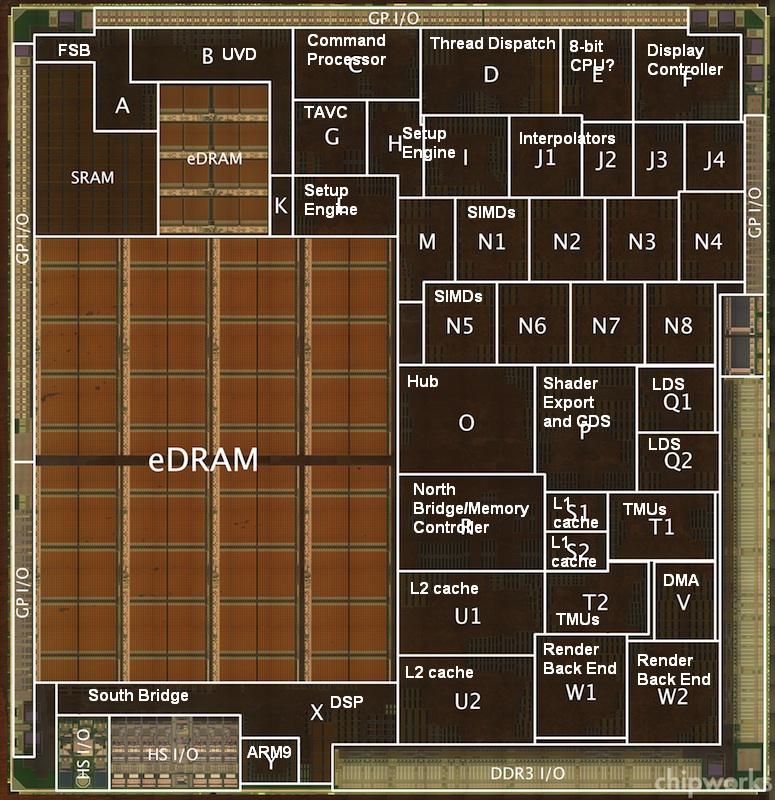
Since I'm back for now and this thread seems like it could get locked at any moment now, I may take some time later and annotate the die photo according to what I've gathered. There are actually very few blocks left unaccounted for once it's all put together.
I wonder what aspects of the Wii U would give the most trouble when porting a game from 360/PS3. Is it more CPU related, or are there any GPU issues. Anyone wanna chime in?
I wonder what aspects of the Wii U would give the most trouble when porting a game from 360/PS3. Is it more CPU related, or are there any GPU issues. Anyone wanna chime in?
Ok, then. What if I told you PPC750cl's 'paired-singles' were more advanced (as in: they were further along the path that SIMD has come over the years) than P3's SSE - what would you call them then?In literal terms, yes, I recon I would call the original SSE SIMD, since that's what it does. But it's not all black or white, that's obviously a more primitive form of SIMD compared to modern implementations.
Ok, then. What if I told you PPC750cl's 'paired-singles' were more advanced (as in: they were further along the path that SIMD has come over the years) than P3's SSE - what would you call them then?
I would guess CPU, for all the reasons discussed. The GPU may take a bit of work to coax good ports out of, but the CPU is a completely different design ideology from the 7G HD twins. Long pipelines and high clocks vs short pipeline and low clocks, in-order with more lanes vs out of order, lots of SIMD (I keep opening up that can of worms, don't I?) vs an older form, very floating point heavy vs weaker FPU in favor of integer performance, etc etc.
 )
)Thanks, glad to see that discussion is starting to get more level-headed over the last page.Glad to see you back Fourth. Good catch, 8 bit *something* CPU, not ARM. And I know Starbuck is not that 8 bit CPU (which is thought to help with Wii-Wii U compat), I wasn't equating the two. He was asking something about how the Starbuck security core could interact with the GPU or something, which was why I had the two separate CPUs in the same paragraph at all.
I probably am. With all the back an forth of ALU, TMU, SP, Shaders, and all the difference names, I sometimes get things mixed up. You should get the gist of what I was suggesting though.
Though, since you mention Starbuck, do we know its clock and power consumption?
Unfortunately, krizzx, some people cannot provide sources. People's jobs are on the line. It would be extremely productive to, instead of dismissing what you perceive as a negative/attack type thing without sources as bunk, to attempt to reason as to why they have that opinion.
As an example, if you disagree with USC-fan (as I have many times in the past, even if I don't necessarily disagree with some of what he's saying right now) you can debate as to why you disagree and present your facts without any sort of antagonistic language or outright dismissal. It may serve the thread for good, quite honestly, to have that type of discussion happen. For the most part, the last couple of pages have been this way.
wsippel is a great example. He has a great amount of knowledge and has a lot of sources in the industry (actually, he's just extremely good at digging - one of the best in this forum), and he says "well maybe it's not so simple as to be a 176gf part. And ______ is why. However, it's also possible that it is such a part. But these metrics aren't necessarily the end-all-be-all because we're seeing so and so in game as efficiency improvements"
Without so much as a whimper of antagonistic language, he presented his opinion on why it could be the case and why it couldn't. That made for a productive back-and-forth with USC-fan, who said "hey, maybe you're right - it's not impossible". That's the kind of discussion that gets people's opinions across, negative and positive, without resorting to any kind of "attacks" - right? It makes for an awesome thread, certainly. We would all be better off dropping talk like "agendas" and extreme viewpoints. If you feel someone has an agenda, instead of saying "you have an agenda!" try debating the person the way wsippel has (i.e. "it's possible you are incorrect, and this is why *insert fact or speculation here*").
edit: and obviously this is directed at the thread in general, not just a single poster, when discussing making this place less of a shitstorm
This may be an unpopular opinion but I think, just judging by the released games, the CPU is somewhat weaker than a 360 (maybe 80% of a 360? Just going by the framerate issues in nearly every port released, reduced player counts even in a "good" port like NFS Most Wanted, also it's known to be much weaker in floating point performance, etc.) and the GPU is maybe 10-20% faster than 360 (just going by released games, we see almost no resolution bumps, even from sub-HD to 720p, but sometimes we see better AA so I think there is a performance delta in favor of the Wii U there, but it ain't much).
Would be interesting to hear what someone who is working on the hardware has to say. I honestly don't really know anyone working on it (that's kind of a bad sign
Well didn't a dev very recently mention its slightly more powerful than an Xbox 360 (Gianna Sisters dev?). If it was 50% more powerful, I don't know if they would have described it that way.

How would a dev accurately measure a percentage increase though?? Slight could mean anything depending on the scale. Let's not get into over-analysing vague comments. It's not that time of the week yet
Well didn't a dev very recently mention its slightly more powerful than an Xbox 360 (Gianna Sisters dev?). If it was 50% more powerful, I don't know if they would have described it that way.
it's a 640:32:16 process... so what if we split that process in half (320:16:8)
What's the point of relating it to the 4770 at all if you're going to cut the configuration down? That would make it an entirely different GPU.
That's like saying the 620M is essentially a 680m...If you cut a bunch of stuff out. I don't see the point.
Well.. use it as a base for the calculation? Seems to sorta fit if you get the process down to something that won't take up as much die space.
But the 4600 series already has 320 shaders
If 320 shaders *is* the right count at all, the 4770 comparison still seems pointless to me if other GPUs in the lineup already match the number without the hacksaw
The whole GPU die is made on the same process, so or it's all 45nm or it's all 40nm.What about a 4770?
It's natively 40nm, it's normally 137ish mm^2(IIRC).
That's obviously too big though... it's a 640:32:16 process... so what if we split that process in half (320:16:8)... take into account the memory controller, etc... you'd have about 70~80mm^2 used up (super rough estimate). Keep in mind 45mm^2 is used up by the eDRAM. That leaves 20-30mm^2 left over for fixed functions and other pieces?
Is that possible? Of course this is all super rough estimates... Idk though.
The 45nm thing could very well happen, we assumed 40 nm because TSMC used that process, it doesn't mean it has to be the same with Latte.Fourth Storm said:We actually don't know how many transistors Latte has. Estimates were drawn up by using the die size and comparing it to 40nm TSMC products. Latte is a Renesas product and may not even be 40nm (I've heard 45nm, which makes alot of sense given their current production lines). Even on the same process node, Renesas transistors may be larger than TSMC's.
The whole GPU die is made on the same process, so or it's all 45nm or it's all 40nm.
But the 4600 series is 55nm.
Thanks for the explanation. It's always good to learn new things!When a fabrication plant says XXnm, that just describes the minimum feature size. Not all transistors have to be that size. Haswell has transistors larger than 22nm for sure, etc etc. And especially across fabrication plants. Intels 22nm appears more dense than 28nm parts than just the transistor size would account for, and even TSMCs 20nm isn't expected to be denser despite the smaller name. There's also layout optimization, you can optimize for power, performance, or die size, and each trades off some of the other two.
Just to clarify. I know what you meant.
The only thing I would ask with my limited knowledge is: isn't the 8-bit CPU on your scheme a bit too big? I mean, how come is it 3 to 4 times bigger than the ARM9 which is a 32 bit CPU?Here's where I'm at with the die presently. I've explained how I've arrived at these IDs in various past posts, which I can dig up if people have questions or want to discuss any of the various block. I am vague with the setup engine, because it's really hard to tell, using the Brazos die photo, which block on Latte is the rasterizer, which is the vertex setup, and which is the geometry setup (if the last two are discreet blocks).
The only block I don't really have a guess on at the moment is M and K, although the latter may be related to the eDRAM on its left.
The only thing I would ask with my limited knowledge is: isn't the 8-bit CPU on your scheme a bit too big? I mean, how come is it 3 to 4 times bigger than the ARM9 which is a 32 bit CPU?
Here's where I'm at with the die presently. I've explained how I've arrived at these IDs in various past posts, which I can dig up if people have questions or want to discuss any of the various block. I am vague with the setup engine, because it's really hard to tell, using the Brazos die photo, which block on Latte is the rasterizer, which is the vertex setup, and which is the geometry setup (if the last two are discreet blocks).
The only block I don't really have a guess on at the moment is M and K, although the latter may be related to the eDRAM on its left.
I'm with Freezamite on the 8-bit CPU thing. That looks a little odd for the size.
Also, what is that small section between M, N5 and O? Its not even labeled like "who cares what this thing is". I asked a long time ago but got no answer. Is it possible that could be the 8 bit CPU? K also looks plausible, and that small segment seems to mirror K little.
Considering Occam's Razor was brought up, I'd like to mention a related rule. Don't remember what it was called, but the basic idea is: The more obvious a solution appears to be, the more likely it's wrong.
Considering Occam's Razor was brought up, I'd like to mention a related rule. Don't remember what it was called, but the basic idea is: The more obvious a solution appears to be, the more likely it's wrong.
Went to the Wiki, and Xenos has 240 Gflops.
Why are people assuming Latte has 176 or whatever? I know the jury's still out on the CPU, but hasn't literally every developer who's made a comparison between latte and xenos say that latte outclasses it (maybe not by a LOT, but still)?
If I had to guess, it's probably "hUMA" anyway, with both CPU and GPU capable of accessing both MEM1 and MEM2. In native mode, MEM0 is managed by the OS according to Marcan. I assume one MEM0 pool might be used as a buffer for CPU-GPU communication, and the other as a buffer for MEM2.Was thinking this before but thought it was too cray cray....But seeing as it's brought up in that link, I'll ask: Is it possible espresso can use eDRAM as a cache? If so then seeing as Latte also accesses it as VRAM - is that not sorta like the hUMA thing from AMD (unified pool of memory)? Would also explain the tenuous link to power 7 (which I know was pr guff, but must have had a shred of a reason to mention it in the first place) as Power7 does something similar with the eDRAM doesn't it?
Like I said, probably crazy but I thought I'd ask.
You can't really compare Latte to any conventional AMD part to begin with. It's not an APU, but it's not a stand-alone GPU, either. There's a ton of stuff on the die you won't find on a regular GPU, but there's also stuff on regular GPUs Latte doesn't have (no GDDR memory controllers for example).I have one niggling question regarding Latte.
Why is it compared to Brazos parts again? I really don't see any sort of resemblance-in-purpose merits. One of them is a low-end APU with a strict TDP budget (shared by necessity between CPU and GPU), the other a highly custom stand-alone GPU with a reasonably generous power budget (for a low-powered part).
I'd find it more accurate were one to compare Latte to AMD's own 40 nm mobile parts from the same era (RV7x0) as the Latte is suspected to originate. Even better if someone would volunteer such a laptop for ritual sacrifice and innards reading by a techno-haruspex.
Was thinking this before but thought it was too cray cray....But seeing as it's brought up in that link, I'll ask: Is it possible espresso can use eDRAM as a cache? If so then seeing as Latte also accesses it as VRAM - is that not sorta like the hUMA thing from AMD (unified pool of memory)? Would also explain the tenuous link to power 7 (which I know was pr guff, but must have had a shred of a reason to mention it in the first place) as Power7 does something similar with the eDRAM doesn't it?
Like I said, probably crazy but I thought I'd ask.
I have one niggling question regarding Latte.
Why is it being compared to Brazos parts again? I really don't see any sort of resemblance-in-purpose merits. One of them is a low-end APU with a strict TDP budget (shared by necessity between CPU and GPU), the other a highly custom stand-alone GPU with a reasonably generous power budget (for a low-powered part).
I'd find it more accurate were one to compare Latte to AMD's own 40 nm mobile parts from the same era (RV7x0) as the Latte is suspected to originate. Even better if someone would volunteer such a laptop for ritual sacrifice and innards reading by a techno-haruspex.
Guys, I found this recently http://playeressence.com/is-the-wii-u-even-powerful-enough-to-handle-gta-v/
This Eyeofcore comes from Gamefaqs and we know this board has a lot of fake.
So is it possible or is it another bullshit thing?