Wolzard
Member
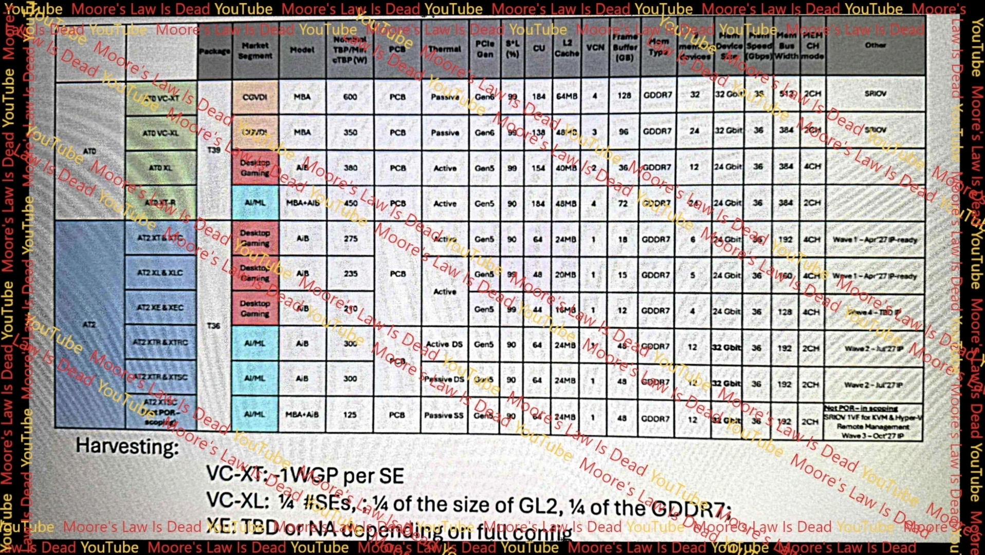
| GPU | Shader Arrays (SA) | Shader Engines (SE) | Compute Units (CU) | Memory Controller (UMC) |
|---|---|---|---|---|
| AT0 GPU | 8 | 16 (2 per SA) | 96 (6 per SE) | 16 (32-bit?) |
| AT0 GPU | 4 | 8 (2 per SA) | 40 (5 per SE) | 6 (32-bit?) |
| AT3 GPU | 2 | 4 (2 per SA) | 24 (6 per SE) | 8 (16-bit?) |
| AT4 GPU | 1 | 2 (2 per SA) | 12 (6 per SE) | 4 (16-bit?) |
AT0 featuring 96 Compute Units, organized into 8 Shader Arrays. Each Shader Array would contain 16 Shader Engines, with every Shader Engine including 6 Compute Units.

AT2 GPU is said to feature 40 Compute Units, with each Shader Engine containing 5 CUs. Its UMC block (memory controller) is estimated at six, suggesting a 192-bit memory bus, while AT0 is expected to use a 512-bit bus.

AT3, meanwhile, is rumored to have 24 Compute Units. Interestingly, it would have more UMCs than AT2 which may come from AT3 and AT4 being designed with LPDDR5X memory, requiring more controllers. The AT4 could have 12 CUs, with each memory controller on these chips believed to be 16-bit wide.


https://videocardz.com/newz/amd-rdn...-gpu-with-512-bit-memory-bus-96-compute-units