Castef
Banned
Some insiders have suggested the gap between Switch and Xbone is less than the gap between Xbone and PS4. Take with a grain of salt though.
Yet, the 4GB gap in RAM is really, really wide.
Some insiders have suggested the gap between Switch and Xbone is less than the gap between Xbone and PS4. Take with a grain of salt though.
If rumors are correct, as far as games are concerned there will be a 2GB difference. Nintendo won't be going with a heavyweight OS.Yet, the 4GB gap in RAM is really, really wide.
3.2GB (720p-1080p) vs 4.5/5/5.5GB (900p-4k).Yet, the 4GB gap in RAM is really, really wide.
Yet, the 4GB gap in RAM is really, really wide.
Well, firstly, if they were targeting Holiday 2016 then they clearly delayed it. Was the delay purely about software? If so, why not take advantage of the cheaper and more efficient manufacturing process anyway? Would they have built these chips months ago and had them sitting in a warehouse all this time?
And again, Maxwell doesn't mean 20nm. They could have chosen Maxwell on 16nm and it would be just as efficient as Pascal. Haven't 16nm processes been available for quite a while? Even possible for a Holiday 2016 launch?
It's very possible the chip design was finalized in 2015. Nvidia had no way to predict how their 16nm products would scale at that time in full production, and they did in fact have supply issues with GeForce Products after launch due to fab constraints.
You can't rule out 16nm, but there's no evidence to support it other than speculation, either. I think people should prepare for this to be pretty much a Tegra X1 in terms of performance and design, with perhaps some light customization to facilitate the dock/TV output and perhaps some cache modifications to overcome the anemic nature of the primary memory interface. That's not necessarily bad. Most of the issues with the X1 were related to Android and it's horrible GL performance. Maybe we'll get lucky and the Switch will have more GPU cores than a standard X1.
The final dev kits being Maxwell is a dead giveaway.
Again, if the chip is 16nm that doesn't suddenly make it Pascal, its still a heavil customised Maxwell with whatever code name that chip has. Nobody's said what the node for the GPU in the final development kit is.
") _/¯
_/¯All true, but Nate did say not much has changed for the final kits, so..... ¯\_(ツ
We don't have any evidence other than every other Maxwell Tegra product being on 20nm. Given that Nintendo was supposedly given a killer deal on chips, perhaps they bought up the remaining 20nm fab commitments from Nvidia? That would explain the 20nm Tegra X1 Shield Tablet disappearing from the roadmap, and the Shield TV channels drying up in anticipation of the 16nm refresh.
Nate also said its Pascal based though didn't he? Unfortunately none of this is revealing. What I'd like to hear from these leakers is plain and simple, what node is it on. Throwing around chip names is irreverent.
No offence meant to Nate BTW, just saying that Maxwell/Pascal really isn't relevant unless you specify that you mean the node is the same.
Nate was the one who had a source that tipped him off to the final devkits being out there. They are Maxwell and not a lot was changed from the previous kits.
I think you're grasping a bit to hold onto the 16nm dream. I think it's best to let it go, and be pleasantly surprised if we hear good news.
If rumors are correct, as far as games are concerned there will be a 2GB difference. Nintendo won't be going with a heavyweight OS.
Nate was the one who had a source that tipped him off to the final devkits being out there. They are Maxwell and not a lot was changed from the previous kits.
I think you're grasping a bit to hold onto the 16nm dream. I think it's best to let it go, and be pleasantly surprised if we hear good news.
how switch will is supposed to do 1080p with 25 gb/s shared bandwidth?
no f way. Xbox 360 has 22gb/s (32gb/s to the edram).
[0419] The main unit 2 includes a cooling fan 96 for radiating heat from inside the main unit 2. With the cooling fan 96 in operation, the air outside the housing 11 is introduced into the housing 11 through the air inlet hole 11d and the air inside the housing 11 is discharged through the air outlet hole 11c, thereby discharging heat from inside the housing 11. The cooling fan 96 is connected to the CPU 81, and the operation of the cooling fan 96 is controlled by the CPU 81. The main unit 2 includes a temperature sensor 95 for detecting the temperature inside the main unit 2. The temperature sensor 95 is connected to the CPU 81, and the detection results of the temperature sensor 95 are output to the CPU 81. The CPU 81 controls the operation of the cooling fan 96 based on the detection results of the temperature sensor 95.
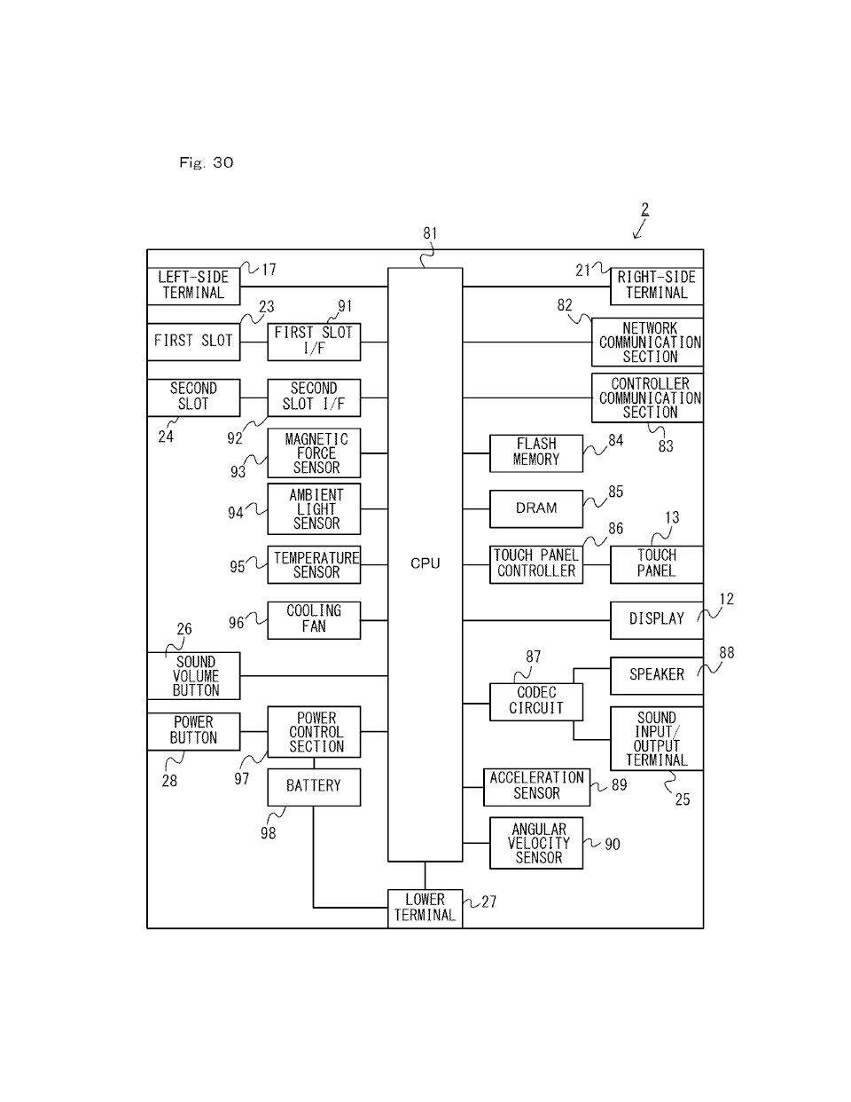
[0556] In the present embodiment, in the portable mode, the operation of the cooling fan 96 is limited. Specifically, in the portable mode, the rotations per minute (rpm) at which the cooling fan 96 is allowed to operate (in other words, the fan speed) is limited to be lower than the highest rpm at which the cooling fan 96 is allowed to operate in the console mode. For example, in the portable mode, the cooling fan 96 is controlled to operate at a predetermined rpm or less, which is lower than the maximum rpm.
In the present embodiment, in the portable mode, the clock frequency range over which the CPU 81 is allowed to operate is limited. In the present embodiment, the clock frequency at which the CPU 81 is allowed to operate can be specified within a predetermined range by the program executed on the main unit 2. In the portable mode, the range over which a clock frequency can be specified by the program is limited as compared with that in the console mode. For example, the range over which a clock frequency can be specified in the console mode is X1 [Hz] or less, whereas it is limited to X2 (<X1) [Hz] in the portable mode. Note that if the main unit 2 includes a GPU (Graphics Processing Unit) in addition to a CPU, the range of processing power (i.e., clock frequency) may be limited for the CPU and/or for the GPU.
In the present embodiment, in the portable mode, the image rendering capacity (which can also be referred to as the image generating capacity) is limited. Specifically, in the portable mode, the resolution (in other words, the number of pixels) of images generated by the main unit 2 is lower than that in the console mode.
how switch will is supposed to do 1080p with 25 gb/s shared bandwidth?
no f way. Xbox 360 has 22gb/s (32gb/s to the edram).
Does it mention a fan in the dock as well?
How does my post have any suggestion of grasping to a dream of 16nm?.. What I'm trying to explain is that these leaks don't tell us anything and people are just wasting their time with the current fuss and obsession with "Its Maxwell" or "Its Pascal". Because by the very nature of Maxwell/Pascal (similarity of the chips and the fact Switch GPU is custom and started development long before Pascal ever came along) trying to decide what the chip will end up as based on the name Maxwell or Pascal is pointless.
If any of these leakers would just make a claim on the node being used, or number of cores, or clock speed it would be worth talking about.
Does it mention a fan in the dock as well?
Every Tegra product based on Maxwell is 20nm. That should be the assumption unless we get decent information that proves otherwise. I agree the obsession with Maxwell or Pascal is off base in some ways because of how similar they are, but it does give us a rough idea of the ballpark we're in when it comes to power consumption and performance expectations. Thraktor's post earlier in this thread outlined how similar performance could be achieved between the two.
The leakers will have no idea what node it's on, because they are getting information second hand from developers or studio insiders who aren't going to be able to pull lithography information from the tools at their disposal.
And this is the main issue right now. Unless the die size is documented, we aren't going to be able to get specifics outside of the architecture the Switch is based upon. Like I said, final dev kits are Maxwell based. Began distribution in November.
The Pascal information I received months ago is from different contacts than the 5-8hr target battery range - remember, this is a range that was being targeted and never a sure thing.
So new news then?
Nothing there is new and it's stuff I've said numerous times before.
Every Tegra product based on Maxwell is 20nm. That should be the assumption unless we get decent information that proves otherwise. I agree the obsession with Maxwell or Pascal is off base in some ways because of how similar they are, but it does give us a rough idea of the ballpark we're in when it comes to power consumption and performance expectations. Thraktor's post earlier in this thread outlined how similar performance could be achieved between the two.
The leakers will have no idea what node it's on, because they are getting information second hand from developers or studio insiders who aren't going to be able to pull lithography information from the tools at their disposal.
She specifically said in a tweet in October that the retail versions will have 4GB of RAM.
https://mynintendonews.com/2016/10/...ntendo-switch-has-4gb-of-ram-in-retail-units/
Denial is the first stage of grief.
And this is the main issue right now. Unless the die size is documented, we aren't going to be able to get specifics outside of the architecture the Switch is based upon. Like I said, final dev kits are Maxwell based. Began distribution in November.
The Pascal information I received months ago is from different contacts than the 5-8hr target battery range - remember, this is a range that was being targeted and never a sure thing.
 .
.Right but knowing the final RAM target is a lot different to knowing the specific chip architecture final hardware will use especially when they are so similar from a performance standpoint anyway whether they go with Maxwell or Pascal.
So you think Emily has access to finished retail hardware ?
All the info info she has is based on devkits.
I personally couldn't give a toss which architecture it uses, I'm buying it to play Nintendo games regardless.
And this is the main issue right now. Unless the die size is documented, we aren't going to be able to get specifics outside of the architecture the Switch is based upon. Like I said, final dev kits are Maxwell based. Began distribution in November.
The Pascal information I received months ago is from different contacts than the 5-8hr target battery range - remember, this is a range that was being targeted and never a sure thing.
Yeah but every Maxwell product is based on 20nm because once they dropped Maxwell to 16nm they called it Pascal to make it sound like it was some great new technology. 20nm can be seen as the worst case scenario, as it always has been.
Did the document specifically mention the fan being active in portable mode?Good to know, thanks. Something is weird about the Switch having an internal fan in the tablet (and apparently not in the dock, though that can be added even if it's not in the patent) yet still reaching 5 hours of battery. I'm not sure if they'll realistically reach that target, but it would only make sense if it is on a 16nm process.
That article sure did cause a Gaf meltdown didn't it...
Did the document specifically mention the fan being active in portable mode?
[0556] In the present embodiment, in the portable mode, the operation of the cooling fan 96 is limited. Specifically, in the portable mode, the rotations per minute (rpm) at which the cooling fan 96 is allowed to operate (in other words, the fan speed) is limited to be lower than the highest rpm at which the cooling fan 96 is allowed to operate in the console mode. For example, in the portable mode, the cooling fan 96 is controlled to operate at a predetermined rpm or less, which is lower than the maximum rpm.
And this is the main issue right now. Unless the die size is documented, we aren't going to be able to get specifics outside of the architecture the Switch is based upon. Like I said, final dev kits are Maxwell based. Began distribution in November.
The Pascal information I received months ago is from different contacts than the 5-8hr target battery range - remember, this is a range that was being targeted and never a sure thing.
Yes, although at a lower RPM than when docked:
Just to be clear, how do you check your sources are legit ? I'm sure you do a better job than just listening to random twitter users who send you private messages
Interesting. I hope this thing doesn't get too noisy while in my hand (or face depending on if Nintendo utilize the VR-like capabilities present in the documents)
[0557] With the limitation (b) above, it is possible to reduce the operation noise of the cooling fan 96. In the portable mode, it is assumed that a user uses the main unit 2 close to the user. In view of this, in the present embodiment, since the operation noise of the cooling fan 96 can be reduced in the portable mode, it is possible to reduce the possibility that the user may feel the operation noise is too loud.
Pascal information was provided by individuals I've worked with for years. The talk of Pascal wasn't limited to only me. Other outlets heard the information as well and most were 99% certain it was happening.
Pascal information was provided by individuals I've worked with for years. The talk of Pascal wasn't limited to only me. Other outlets heard the information as well and most were 99% certain it was happening.
Emily seems to disagree with you on this one though.
What I want to know is why people are taking this crazy article as fact? It's like if an article is published, it must be true kinda thing. Is there something about this that warrants believing it?
Sorry but what's the better option ? Maxwell or Pascal ? (makes me think of Tales of series...)
What I want to know is why people are taking this crazy article as fact? It's like if an article is published, it must be true kinda thing. Is there something about this that warrants believing it?
The final dev kits are Maxwell.
Why would that be the case if it's cheaper to go 16nm?
He then compares that 1TF number to the FP32 numbers of the PS4 and Scorpio, and then says that the Switch might be more powerful than the XB1, so who the hell knows what he's basing that on. Most of his conclusions are contradictory nonsense.