Duckhuntdog
Member
Fafalada said:? What are those Xenon features that make it more rich then the PS3 who doesn't have them?
Bill Gates bank roll?
Fafalada said:? What are those Xenon features that make it more rich then the PS3 who doesn't have them?
iapetus said:Depends how high their screen resolution is. Eclipse is a bit ugly to work with on anything less than 1600 x 1200.
rastex said:Eclipse is good with Java, and has gotten A LOT better in C++. It still has a long way to go though in terms of the fancy features. And I'm uncertain how Eclipse handles other repository systems outside of CVS.
 .
.") .
.Well as soon as I get a monitor that can refresh at 100+hz in that res I'll be ok with it then. Can you believe that in this age and day, CRTs capable of that virtually don't exist?Iapetus said:Depends how high their screen resolution is. Eclipse is a bit ugly to work with on anything less than 1600 x 1200.
Panajev2001a said:Something tells me SCEA is hard at work on Subversion
AFAIK, RDRAM's latency problems were exaggerated by the memory interface to the Intel chips. The EE had the mem controller on-chip, so it fared much better. Anyway, the memory system being used here will clown anything on the PC side...period. PEACE.Ryudo said:Rambus ? Nice high bandwidth but sucky high latency as well, at least that was what it was like when it was first released.
rastex said:Eclipse is good with Java, and has gotten A LOT better in C++. It still has a long way to go though in terms of the fancy features. And I'm uncertain how Eclipse handles other repository systems outside of CVS.
DonasaurusRex said:The interesting thing is that you could feasibly put a PCIe card with a cell chip on it and use it as a general co processor tee hee. Some people are saying that the CELL wont perform very well in serial applications due to the lack of main memory access. We'll see. No matter who loses we win , i think processing power for the masses is about it explode.
Panajev2001a said:I am a bit less worried about the compiler, the quality of the other development tools and the documentation: might it be that having IBM helps SCE/Sony and Toshiba in the job of producing nice PlayStation 3 SDK's ?
PCI Express doesn't share its bandwidth like PCI. Each lane has 2.5Gbps dedicated bandwidth in each direction.HokieJoe said:I'm sure that's possible. The only problem it will bump up against is oversaturation of the PCI bus. Remember, you've got lot's of other things running on that bus as well.
soundwave05 said:So is that it for CELL announcements? No fancy Ridge Racer girl or rubber ducky tech demos?
Not really. We still have no idea what the actual specs for the PS3 chipset are. This whole discussion is just a product roadmap for the cell architecture. You're not going to see the same component in DVD player as in a workstation.GhaleonEB said:Okay the bar has been set. Get hopping, MS.")
Panajev2001a said:Uhm... I disagree, it is much worse to have a good CPU paired with a super-super GPU than the opoosite: rendering is not all you do
J2 Cool said:BUT WHAT DOES IT ALL MEAN!?

PS3 CPU should be doing most if not all of the vertex processing - so that kinda involves it in the renderingNo, its not all you do - but there is a ratio such that you have a lot of CPU that's sitting around idle most of the time. Since the CPU isn't apparently not involved in any rendering at all, at most its doing is scene graph management, physics, sound, etc. I wouldn't want cray supercomputer power to do those tasks - it would be wasted.

Well I kinda agree - It both improves and breaks things from 6, so it's really a mixed bagVS.NET has gotten a bit too 'feature rich' for my liking. I preferred the VS6 IDE but the compiler wasn't standards compliant. The VS7 compiler is better but the IDE is a monstrosity.
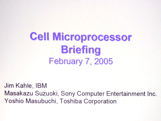
border said:Okay so the Sony Cell presentation is going on right now.....are there any sites planning to have up-to-the-minute coverage?
Has OpenGL ES actually been confirmed as being a part of the PS3 toolchain or are we still making assumptions about the toolchain?
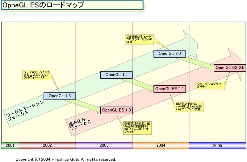
Andrew2 said:It will be as OpenGL ES 2.0 would be introduced this year:
http://pc.watch.impress.co.jp/docs/2004/0729/kaigai104.htm
Secondly,SCEI didn't join the Khronos group for no reason
TAJ said:With a powerful enough CPU, you wouldn't need 3D acceleration. Software renderers are much, much better than hardware-accelerated ones, anyway.
Andrew2 said:It will be as OpenGL ES 2.0 would be introduced this year:
http://pc.watch.impress.co.jp/docs/2004/0729/kaigai104.htm
Secondly,SCEI didn't join the Khronos group for no reason
soundwave05 said:So is that it for CELL announcements? No fancy Ridge Racer girl or rubber ducky tech demos?
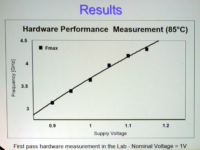
Pimpwerx said:That's nothing really. The beauty of the architecture lies in its scalability and software hierarchy. The power gains are made to come from stacking PEs. So some of the fud from today is that the PS3 will probably see 2 of these cores (PEs) in its CPU. That would be pretty badass IMO. But we'll see how they solve the powerhandling problems. People wigged out at the 85C temp, but I thought that was without a fan. I assume there was a heatsink, or something like it though. We'll see.
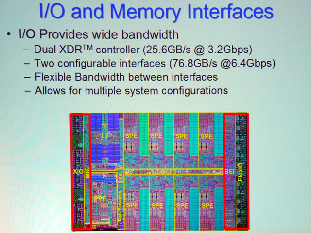
Oh yeah, Rambus gets a lot of stick for a company that's still developing great new products. 100GB/s? :O That's just bananas. External bandwidth is really picking up.


HyperionX said:
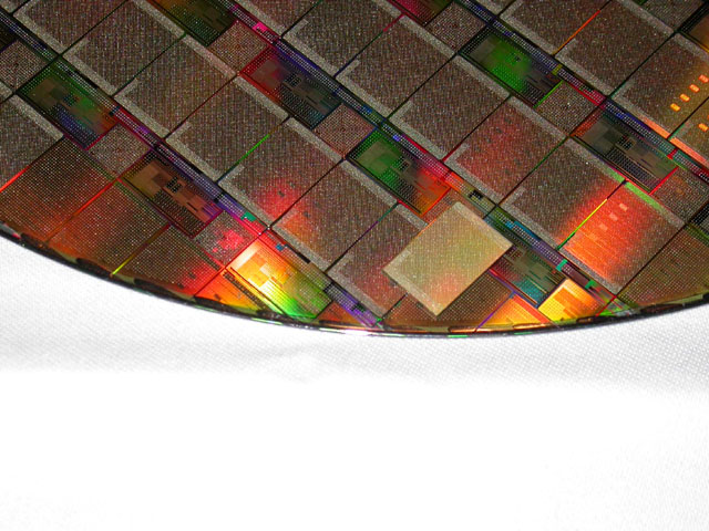
Looks like Cell is dual-core plus extra (eDRAM?) in this shot. However, that's one focking big ass die, like 600m^2-700mm^2. This is ridiculously large and I'm guessing it's some sort of developement or testing chip on the wafer and the actual production chip is the separate one on top.
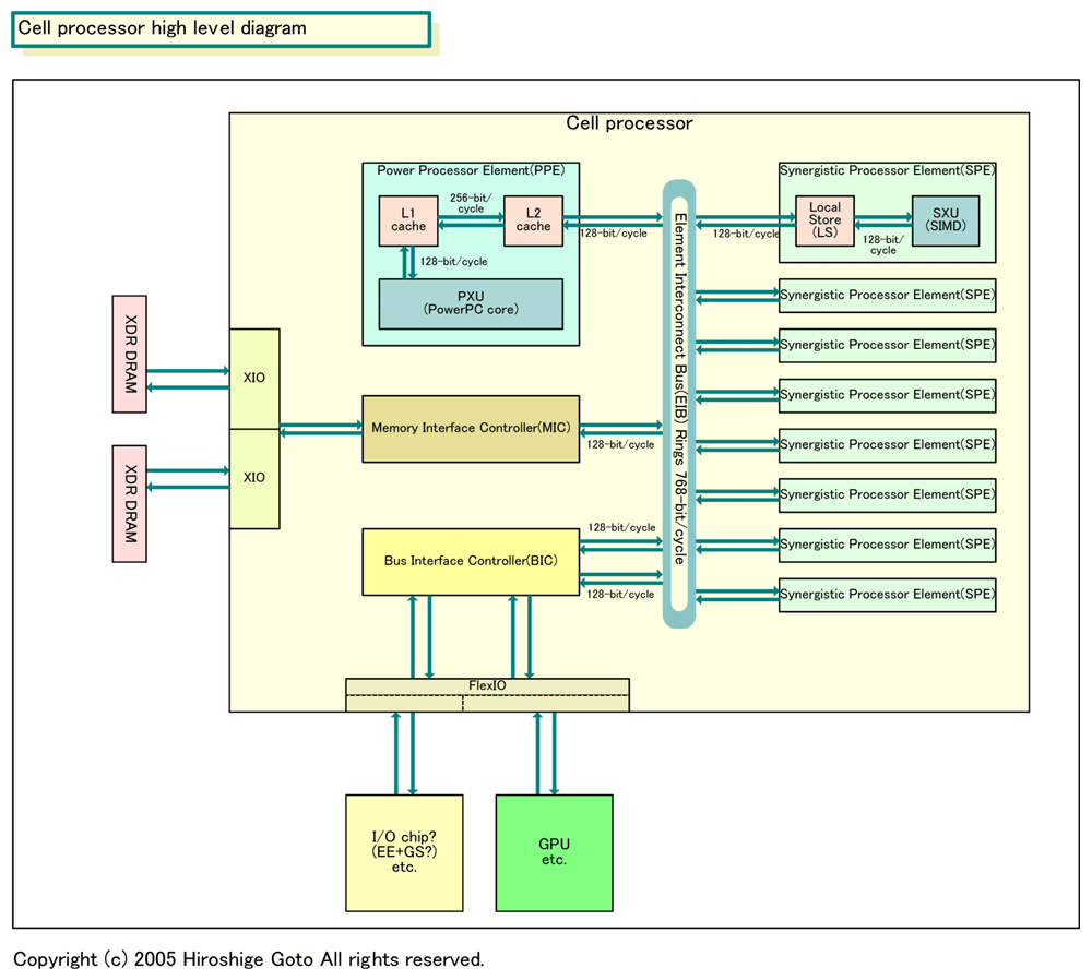
This RAM functions in the role of the L1 cache, but the fact that it is under the explicit control of the programmer means that it can be simpler than an L1 cache. The burden of managing the cache has been moved into software, with the result that the cache design has been greatly simplified.
The difference is that instead of the compiler taking up the slack (as in RISC), a combination of the compiler, the programmer, some very smart scheduling software, and a general-purpose CPU doing the kind of scheduling and resource allocation work that the control logic used to do.
All loop unrolling is done by the programmer/compiler
Wario64 said:For chrissakes, aren't you mods gonna stop him? Although it was funny when he requested someone to make a thread for him, hahah
Sony chip to transform video-game industry
TECHNOLOGY ENVISIONS ALL-IN-ONE BOX FOR HOME
By Dean Takahashi
Mercury News
Sony's next-generation video-game console, due in just two years, will feature a revolutionary architecture that will allow it to pack the processing power of a hundred of today's personal computers on a single chip and tap the resources of additional computers using high-speed network connections.
If key technical hurdles are overcome, the ``cell microprocessor'' technology, described in a patent Sony quietly secured in September, could help the Japanese electronics giant achieve the industry's holy grail: a cheap, all-in-one box for the home that can record television shows, surf the Net in 3-D, play music and run movie-like video games.
Besides the PlayStation 3 game console, Sony and its partners, IBM and Toshiba, hope to use the same basic chip design -- which organizes small groups of microprocessors to work together like bees in a hive -- for a range of computing devices, from tiny handheld personal digital assistants to the largest corporate servers.
If the partners succeed in crafting such a modular, all-purpose chip, it would challenge the dominance of Intel and other chip makers that make specialized chips for each kind of electronic device.
``This is a new class of beast,'' said Richard Doherty, an analyst at the Envisioneering Group in Seaford, N.Y. ``There is nothing like this project when it comes to how far-reaching it will be.''
Game industry insiders became aware of Sony's patent in the past few weeks, and the technology is expected to be a hot topic at the Game Developers Conference in San Jose this week. Since it can take a couple of years to write a game for a new system, developers will be pressing Sony and its rivals for technical details of their upcoming boxes, which are scheduled to debut in 2005.
Ken Kutaragi, head of Sony's game division and mastermind of the company's last two game boxes, is betting that in an era of networked devices, many distributed processors working together will be able to outperform a single processor, such as the Pentium chip at the heart of most PCs.
With the PS 3, Sony will apparently put 72 processors on a single chip: eight PowerPC microprocessors, each of which controls eight auxiliary processors.
Using sophisticated software to manage the workload, the PowerPC processors will divide complicated problems into smaller tasks and tap as many of the auxiliary processors as necessary to tackle them.
``The cell processors won't work alone,'' Doherty said. ``They will work in teams to handle the tasks at hand, no matter whether it is processing a video game or communications.''
As soon as each processor or team finishes its job, it will be immediately redeployed to do something else.
Such complex, on-the-fly coordination is a technical challenge, and not just for Sony. Game developers warn that the cell chips do so many things at once that it could be a nightmare writing programs for them -- the same complaint they originally had about the PlayStation 2, Sony's current game console.
Tim Sweeney, chief executive of Epic Games in Raleigh, N.C., said that programming games for the PS 3 will be far more complicated than for the PS 2 because the programmer will have to keep track of all the tasks being performed by dozens of processors.
``I can't imagine how you will actually program it,'' he said. ``You do all these tasks in parallel, but the results of one task may affect the results of another task.''
But Sony and its partners believe that if they can coordinate those processors at maximum efficiency, the PS 3 will be able to process a trillion math operations per second -- the equivalent of 100 Intel Pentium 4 chips and 1,000 times faster than processing power of the PS 2.
That kind of power would likely enable the PS 3 to simultaneously handle a wide range of electronic tasks in the home. For example, the kids might be able to race each other in a Grand Prix video game while Dad records an episode of ``The Simpsons.''
``The home server and the PS 3 may be the same thing,'' said Kunitake Ando, president and chief operating officer of Sony, at a recent dinner in Las Vegas.
Sony officials said that one key feature of the cell design is that if a device doesn't have enough processing power itself to handle everything, it can reach out to unused processors across the Internet and tap them for help.
Peter Glaskowsky, editor of the Microprocessor Report, said Sony is ``being too ambitious'' with the networked aspect of the cell design because even the fastest Internet connections are usually way too slow to coordinate tasks efficiently.
The cell chips are due to begin production in 2004, and the PS 3 console is expected to be ready at the same time that Nintendo and Microsoft launch their next-generation-game consoles in 2005.
Nintendo will likely focus on making a pure game box, but Microsoft, like Sony, envisions its next game console as a universal digital box.
A big risk for Sony and its allies is that in their quest to create a universal cell-based chip, they might compromise the PS 3's core video-game functionality. Chips suitable for a handheld, for example, might not be powerful enough to handle gaming tasks.
Sony has tried to address this problem by making the cell design modular; it can add more processors for a server, or use fewer of them in a handheld device.
``We plan to use the cell chips in other things besides the PlayStation 3,'' Ando said. ``IBM will use it in servers, and Toshiba will use it in consumer devices. You'd be surprised how much we are working on it now.''
But observers remain skeptical. ``It's very hard to use a special-purpose design across a lot of products, and this sounds like a very special-purpose chip,'' Glaskowsky said.
The processors will be primed for operation in a broadband, Net-connected environment and will be connected by a next-generation high-speed technology developed by Rambus of Los Altos.
Nintendo and Microsoft say they won't lag behind Sony on technology, nor will they be late in deploying their own next-generation systems.
While the outcome is murky now, analyst Doherty said that a few things are clear: ``Games are the engine of the next big wave of computing. Kutaragi is the dance master, and Sony is calling the shots.'
