winjer
Member

TSMC to Begin N2 Volume Production Before Year-End
TSMC announced today that its next-generation N2 node will enter series production before year's end, with a rapid ramp planned through 2026. This is the second 2 nm-class node to achieve high-volume manufacturing, with Intel's 18A node being the first. Last week, Intel confirmed that its Fab 52...
TSMC announced today that its next-generation N2 node will enter series production before year's end, with a rapid ramp planned through 2026. This is the second 2 nm-class node to achieve high-volume manufacturing, with Intel's 18A node being the first. Last week, Intel confirmed that its Fab 52 is already pushing out 18A wafers in high-volume manufacturing capacity. The TSMC N2 milestone arrives as the manufacturer posted exceptionally strong Q3 financial results, showing that demand for the most advanced chips is moving faster than the industry can add new capacity. Revenue for Q3 was $33.10 billion, reflecting a 40.8% year-on-year gain and a 10.1% quarter-on-quarter increase.
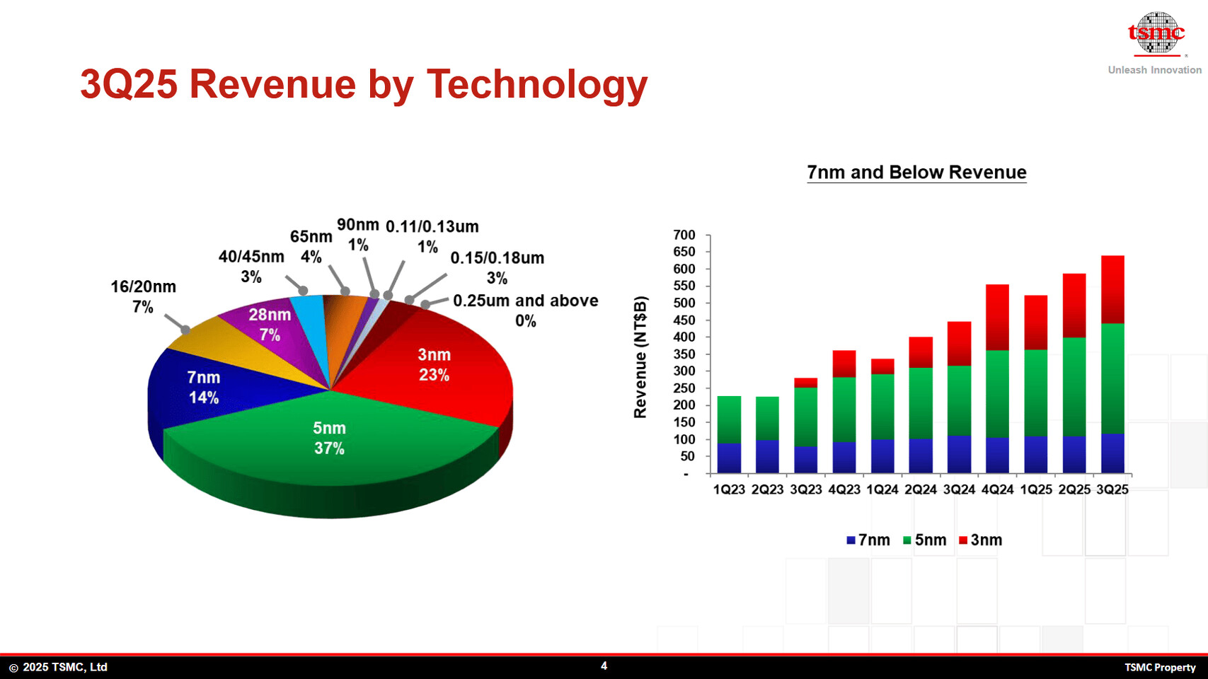
n the third quarter, TSMC processed an astonishing 4.085 million 300 mm wafers, a rise of approximately 22.4% compared to the same period a year earlier, and reported year-over-year revenue growth of nearly 41%, producing roughly $33.1 billion in sales and more than $15 billion in profit for the quarter. Revenue from advanced process families, including all variants of N3, N5, and N7, now accounts for approximately 74% of total sales. By each node, N3 process shipments accounted for 23% of wafer revenue, N5 for 37% and N7 for 14%. The N5 family showed the largest sales increase, reflecting intense demand for AI accelerators and other high-end devices. It is also worth noting that each node carries a different pricing strategy, with newer nodes being significantly more expensive due to the more advanced and involved manufacturing techniques going into them.
TSMC is reinvesting heavily to close the gap between demand and supply. Last quarter, CAPEX reached $9.7 billion, and 2025 spending could total about $42 billion, with roughly 70% earmarked for new fabs and capacity and the remainder for specialties and packaging. The Arizona Fab 21 campus is being expanded and may host future N2 production phases, while an optimized N2P process is planned for the second half of 2026. Even with faster buildouts and outside packaging partners joining the effort, company leaders caution that capacity will likely remain tight through 2026 as customers continue to compete for allocations
Samsung to Receive Two ASML High-NA EUV Lithography Machines for 2nm and DRAM Production
Samsung is advancing its semiconductor manufacturing capabilities with the upcoming installation of two High-NA EUV lithography systems from ASML, scheduled to be operational in the first half of 2026. This move builds upon the company's earlier deployment of the TWINSCAN EXE:5000 research system at its Hwaseong facility, which has been used for early testing and process development. With the addition of the mass-production-oriented TWINSCAN EXE:5200B tools, Samsung aims to accelerate its transition to next-generation nodes.
TrendForce reports that the first EXE:5200B unit will arrive at Samsung's foundry later in 2025, while a second is expected in early 2026. The EXE:5200B represents ASML's first commercially ready High-NA EUV platform capable of supporting volume production. This model follows earlier prototype deployments by Intel in 2023 and TSMC in mid-2024. SK Hynix also installed the same system at its M16 facility for advanced DRAM production last month, indicating growing momentum behind the technology.
Samsung's adoption of High-NA EUV will play a central role in its 2nm process roadmap. Sources suggest the company plans to leverage the new lithography systems to manufacture the Exynos 2600 SoC and Tesla's next-generation AI accelerator. The same tools will also enable Samsung's memory division to develop DRAM featuring vertical channel transistor (VCT) technology, which is expected to replace current planar transistor designs in upcoming nodes.
Each TWINSCAN EXE:5200B system carries an estimated cost of around $386 million, bringing the total investment to approximately $773 million. While the figure underscores the steep expense of High-NA EUV adoption, the technology offers significant advantages — including finer patterning, higher transistor density, and improved yields at sub-2nm geometries.
The new machines are designed to provide higher resolution imaging through a 0.55 numerical aperture optical system, compared to 0.33 NA in previous EUV generations. This enhancement allows for smaller feature sizes with fewer multi-patterning steps, reducing process complexity and improving productivity.
For the first time in a long, long time, we might actually see 3 companies competing at a high-end process node.
And if Intel, TSMC and Samsung start lowering prices to get contracts, and get enough volume production, it might even benefit mere mortal consumers, such as gamers. Let's hope things improve a bit.
