geordiemp
Member
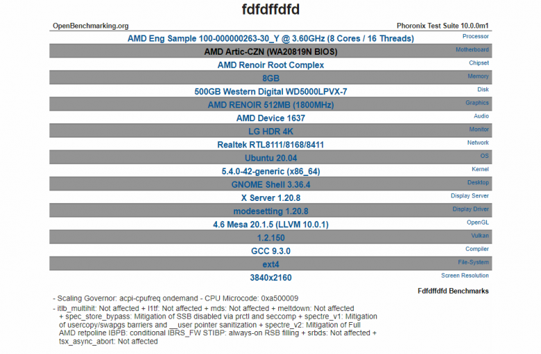
If it was a unified L3 cache a core would have access to 8MB cache rather than 4MB, so you'd have 8MB data width at roughly the same ~20ns as 4MB rather than ~90ns (i.e. you have 50% of your data in L3 and half in RAM).
And what evidence is there that the 2 Ghz test chip with no RT or any other features is the final ps5 APU silicon ?
Github is old, silicon gets revisions, basing everythng of old data is like basing everyhing off old dev kits.


