The Abominable Snowman
Member
Why is he assuming both are TSMC? We know the U GPU is not already. I think even on the same process, one could be smaller per feature if it was gate-first like IBMs fabs.
Earlier analysis from ChipWorks. Its possible they made a mistake but... IDK
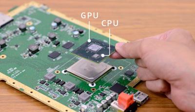
What am I looking at?
The die is exactly 11.88 x 12.33mm (146.48mm²). It's manufactured at 40nm, apparently on an "advanced CMOS process at TSMC". It carries Renesas die markings, but no AMD die markings (although there is an AMD marking on the MCM heat-spreader). This is unexpected, as it was widely reported that the GPU was originally based on AMD's R700 line, and Nintendo publicly referred to it as a Radeon-based GPU. As the die appears to be very highly customised (it looks very different to other R700-based GPUs), the markings (or lack thereof) may indicate that the customisations were not done by AMD, but rather by Nintendo and Renesas.
In addition to the usual GPU components, the die includes a large eDRAM pool (accessible to both CPU and GPU), and it is understood that one or more ARM cores are also on-die, as well as a DSP.

")
")

