WiiU "Latte" GPU Die Photo - GPU Feature Set And Power Analysis

Status
Not open for further replies.
Why is he assuming both are TSMC? We know the U GPU is not already. I think even on the same process, one could be smaller per feature if it was gate-first like IBMs fabs.

Earlier analysis from ChipWorks. Its possible they made a mistake but... IDK

What am I looking at?

The die is exactly 11.88 x 12.33mm (146.48mm²). It's manufactured at 40nm, apparently on an "advanced CMOS process at TSMC". It carries Renesas die markings, but no AMD die markings (although there is an AMD marking on the MCM heat-spreader). This is unexpected, as it was widely reported that the GPU was originally based on AMD's R700 line, and Nintendo publicly referred to it as a Radeon-based GPU. As the die appears to be very highly customised (it looks very different to other R700-based GPUs), the markings (or lack thereof) may indicate that the customisations were not done by AMD, but rather by Nintendo and Renesas.

In addition to the usual GPU components, the die includes a large eDRAM pool (accessible to both CPU and GPU), and it is understood that one or more ARM cores are also on-die, as well as a DSP.
 
Earlier analysis from ChipWorks. Its possible they made a mistake but... IDK

Actually, Jim from Chipworks sent me a followup message stating that 40nm was just his guys' assessment by looking at it. There's no confirmation. OP should probably be updated.

Sorry for any confusion. I thought I had forwarded this info on before, but perhaps I was not clear.

My current speculation is that it is in fact 40nm (eDRAM density makes a great case for this), but might have been fabbed at Renesas' plant - not TSMC.
 
Nintendo might just have "vysnc must be enabled" as part of their lot check requirements. Besides the DS I think Rendition chips back near the dawn of time were the only hardware using a span buffer.
That would seem like a possible if strange explanation. At this point, I'd say a technical reason is more likely.

Also, as I wrote, the DS GPU is a bit of a mystery. It was supposedly developed by a start-up company named Alchemy (which isn't all that surprising for Nintendo, considering they also worked with ArtX and DMP), which was later bought by one of the big guys in the embedded market - I think it was Broadcom. Anyway, Nintendo owns a lot of their tech as far as I know. Maybe they used some of it here?
 
Actually, Jim from Chipworks sent me a followup message stating that 40nm was just his guys' assessment by looking at it. There's no confirmation. OP should probably be updated.

Sorry for any confusion. I thought I had forwarded this info on before, but perhaps I was not clear.

My current speculation is that it is in fact 40nm (eDRAM density makes a great case for this), but might have been fabbed at Renesas' plant - not TSMC.

It's a tweaked HD5550. The card and its powerdraw etc are just too good a fit. Everything about it is pretty much spot on to what we think we know.
 
WiiU will be manufactured way beyond 2015.


This is negative PR only in the eyes of the people looking for negative nintendo PR.

A good deal of the engines and titles running on Orbis/Durango will be running on tablets and smartphones. WiiU has no technological issue there.

Would something like Watch_Dogs be possible on a tablet ?.
 
Watch_Dogs is cross gen already. Im pretty sure it's possible to run on Wii U and will be possible on iPhone 8.

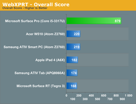
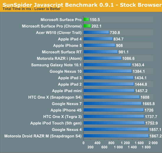
By happy coincidence, Anandtechs Surface Pro review shows just how many times more powerful even ULV (ultra low voltage) processors still are over ARM ones like in the iPhone.

52972.png


52955.png


And graphics performance is probably even larger a leap.

Granted, if it's running on 7 year old consoles it probably can scale back quite a bit, but I'm thinking by iPhone 8 is optimistic.

And yes I probably put too much thought into your probably off the cuff remark :P

Edit: on the other hand, by the SGX Rogue/600 series mobile GPUs, mobile ARM SoCs graphics components will be comparable in raw FLOPS to the 360 at just over 200...Hmm. I don't think the Cortex A15 is close to the PS360 processors still though.
 
By happy coincidence, Anandtechs Surface Pro review shows just how many times more powerful even ULV (ultra low voltage) processors still are over ARM ones like in the iPhone.

So powerful it needs a fan. In a tablet.

My current speculation is that it is in fact 40nm (eDRAM density makes a great case for this), but might have been fabbed at Renesas' plant - not TSMC.

Weren't we already told that the die has the mark from Renesas (or was that for the CPU) so it is indeed fabbed by them? Kind of surprised that TSMC even came into the picture for this.
 
A few comments:

Patent

I had a quick read through the patent posted earlier in the thread, and I'm afraid I'm pretty sure it's about Wii, not Wii U. The diagrams match Wii (e.g. Texture Environment Unit), and the examples given all match perfectly to Wii (such as repeated references to 1T-SRAM, and use of 3.2GB/s as a bandwidth, which I'm pretty sure corresponds to the bandwidth for a particular Wii component). It's interesting, but it doesn't seem to be anything new for Wii U.

eDRAM vs. 1t-SRAM

While there's been a bit of debate over whether the pools are eDRAM or 1T-SRAM, I'm leaving it as eDRAM in the OP for the following reasons:

- Chipworks identified both pools as eDRAM
- Nintendo's internal literature refers to eDRAM for MEM1
- MoSys apparently confirmed that there is no 1T-SRAM used in Wii U
- eDRAM and 1T-SRAM are quite similar technologies, so it wouldn't be surprising for someone to mistake eDRAM for 1T-SRAM, both visually and in their operating characteristics

I think that's sufficient evidence to refer to both MEM1 and MEM0 as eDRAM.

Location of DDR3 bus

This is a point I'm fully willing to consider alternate views on, but again I'm going to leave the info as it is in the OP. I do this pretty much entirely by deference to Chipworks on the matter. As a non-expert myself, I feel my best course of action is to consider the advice of experts, and Chipworks have specifically identified the lower right of the chip as the location of the DDR3 interface. DDR interfaces are probably one of the most common components that Chipworks come across, so I don't see any reason to believe they would be incorrect on this matter.

Potential ROP-less architecture

I find this very interesting, and hope to comment on it (and a few things related to it) in due course.

Edit: I've also made some small edits to the OP, and I've added Marcan's annotated die photo in there too.

Second edit: I figure the interconnect discussion should be more informed when we get the CPU die shot. Whichever interconnect interfaces with the CPU should have a matching one on the CPU die itself.
 
So powerful it needs a fan. In a tablet.

And? My point was a commentary on how far behind ARM processors in phones and tablets still are in raw performance, responding to the guy who thinks they'll run Watch Dogs soon-ish. Whether it takes a fan or twenty to get there is irrelevant to how much forward ARM processors have to come to get there.

And it's more comparable to a Macbook Air than other tablets, bearing in mind this runs full Windows and a full Core i5 proc. And those certainly need fans. But again my point wasn't to defend the Surface Pro.


This addition to the OP was interesting:
https://twitter.com/marcan42/status/298922907420200961

Why would the 1MB SRAM not be available in Wii U mode? Brings me back to maybe it being used to make CPU-GPU cross talk faster (as copy to main RAM penalties often are more time consuming than the operation on the GPU itself). We don't *KNOW* that it's not available, still just speculation. But I'd wonder why there is three distinct pools of memory.
 
It just makes much better sense of things having the DDR3 and CPU I/Os switched from what we initially thought.

Holy crap. I actually said that ages ago in this thread! Ok, my reasoning was just the physical location of the cpu in relation to the gpu on the mcm package (it's bottom right of gpu) but still! First time I've been right on gaf - even it it was by fluke! I'm taking that.

I must be a closet genius!


Edit. Composed myself now. This is what I meant though:

wii-u-GPU-and-CPU.jpg


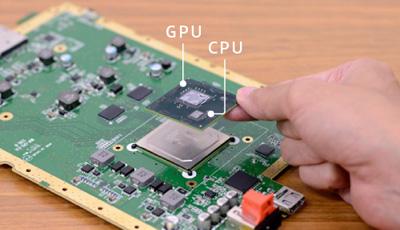
Looking at the physical location of the DDR3 RAM (above and to the left of the MCM) and the CPU (lower right of the GPU on the MCM) - why would the I/O for each on the gpu be in the exact opposite corners? Might be a simple explanation, but I'm a layperson :)
 
Idle speculation time: If the ARM chip sits on the south end (Y), then what in all hell is D? It has a humongous amount of SRAM. Plus, that size.
 
Holy crap. I actually said that ages ago in this thread! Ok, my reasoning was just the physical location of the cpu in relation to the gpu on the mcm package (it's bottom right of gpu) but still! First time I've been right on gaf - even it it was by fluke! I'm taking that.

I must be a closet genius!


Edit. Composed myself now. This is what I meant though:

wii-u-GPU-and-CPU.jpg


Looking at the physical location of the DDR3 RAM (above and to the left of the MCM) and the CPU (lower right of the GPU on the MCM) - why would the I/O for each on the gpu be in the exact opposite corners? Might be a simple explanation, but I'm a layperson :)

How do we know the photo we have is oriented in the same way as that photo there? The Latte die is pretty close to being square, so we don't really have any way of knowing how it's oriented on the MCM.

Perfect place for some L2 cache. About the right size too...

Too much logic for a cache, if you ask me, not to mention the complex layout. Block V looks more like a cache to me.
 
How do we know the photo we have is oriented in the same way as that photo there? The Latte die is pretty close to being square, so we don't really have any way of knowing how it's oriented on the MCM.


Too much logic for a cache, if you ask me, not to mention the complex layout. Block V looks more like a cache to me.


I suppose we don't. I had just been assuming that all along as all the exterior shots were oriented that way. I'm not sure why they'd take the high res shots differently but like u say, no way of knowing.

*back into my hole I go*
 
Too much logic for a cache, if you ask me, not to mention the complex layout. Block V looks more like a cache to me.

There is alot going on in Block D. But that is a major chunk of SRAM (64-96kb by my estimation and based on Marcan's identifying the similarly sized chunk on bottom). We have to think what it could be used for. I'm wondering if it's not the L2 integrated w/ the DDR3 memory access controller. If Marcan is correct (and IMO he is), then it seems they integrated the DSP right into the North Bridge - it's not its own block.
 
I suppose we don't. I had just been assuming that all along as all the exterior shots were oriented that way. I'm not sure why they'd take the high res shots differently but like u say, no way of knowing.

*back into my hole I go*

Hey, I'm with you on this one! Come back, I need supporters! lol

Anyway, this pic is much better at making the point. You can see the chip is slightly taller than it is wide.

http://guide-images.ifixit.net/igi/gqSDvioKMCE2DKCr.large

(we're not allowed to just post that image here, are we?)
 
There is alot going on in Block D. But that is a major chunk of SRAM (64-96kb by my estimation and based on Marcan's identifying the similarly sized chunk on bottom). We have to think what it could be used for. I'm wondering if it's not the L2 integrated w/ the DDR3 memory access controller. If Marcan is correct (and IMO he is), then it seems they integrated the DSP right into the North Bridge - it's not its own block.
Disclaimer: I am not a chip designer and/or reverse engineer. Very much not so.

That said, would it really make sense to merge a custom (?) DSP into a (likely) off-the-shelf DDR interface? I mean, you really don't want to fuck up the memory interface. Plus, a DSP likely doesn't really need low-latency memory access of the kind that it'd be integrated into a memory controller, right?

...what does it do, anyway? Camera/Mic related number crunching from the pad, plus audio out device for the WiiU itself? Maybe some NFC stuff too?

I wish i had some DDR knowledge. Still so confused that Narcan and Chipworks can't agree about GPIOs and memory interface distribution. We need to sort that out.

...could it be the GPU master control/DMA engine chip?
 
Hey, I'm with you on this one! Come back, I need supporters! lol

Anyway, this pic is much better at making the point. You can see the chip is slightly taller than it is wide.

http://guide-images.ifixit.net/igi/gqSDvioKMCE2DKCr.large

(we're not allowed to just post that image here, are we?)

So i see you among others have been questioning the fab process again on B3D? Where do you (plural) stand at the moment?

Also, was there never a confirmation or indication that a 40nm process would be used, other than the x-ray?
 
Disclaimer: I am not a chip designer and/or reverse engineer. Very much not so.

That said, would it really make sense to merge a custom (?) DSP into a (likely) off-the-shelf DDR interface? I mean, you really don't want to fuck up the memory interface. Plus, a DSP likely doesn't really need low-latency memory access of the kind that it'd be integrated into a memory controller, right?

...what does it do, anyway? Camera/Mic related number crunching from the pad, plus audio out device for the WiiU itself? Maybe some NFC stuff too?

I wish i had some DDR knowledge. Still so confused that Narcan and Chipworks can't agree about GPIOs and memory interface distribution. We need to sort that out.

...could it be the GPU master control/DMA engine chip?

Well, I'm far from a chip designer myself - no need for apologies. This is just a ton of fun for me. :)

It's very hard to say how they are dealing with memory access in this design. As is evident, there are multiple banks of differing types of memory and the GPU is acting as the hub.

In R700 GPUs, the memory controllers are tightly coupled with L2 cache. This helps reduce latency. My suggestion is that Nintendo might have taken it one step further in block D by integrating the L2 cache with a single DDR3 memory controller (since it's only a 64-bit bus we're talking).

It's admittedly a bit hard to reconcile this with Flipper's design, which integrates the CPU interface, video interface, memory controller, and I/O interface into its "North Bridge" block. Then again, I don't know how much Hollywood changed this design, as it added the ARM core in to the mix as well as necessary circuitry for the USB, FLASH, etc. It also added GDDR3 to the mix. If we had a Hollywood die shot to compare against, I reckon many things would be made clear.

In sum, it's still a mystery how the CPU accesses RAM. Is there one super memory controller that interfaces with both the 32 MB eDRAM and 2 GB DDR3? Are there separate memory controllers for the two different RAM types? My hunch is that Nintendo mean for MEM1 to be the primary pool for the CPU tasks in terms of running game code, such as AI, which benefits from the decreased latency more so than having a high bandwidth. The major task for MEM2 - the DDR3 - would theoretically be to send textures to the GPU.

So i see you among others have been questioning the fab process again on B3D? Where do you (plural) stand at the moment?

Also, was there never a confirmation or indication that a 40nm process would be used, other than the x-ray?

No confirmation. I still think it's 40nm, although they are doing some very interesting comparisons over there. Stay tuned! :)
 
From a less technical viewpoint I talked about lighting, but from a more technical view I wonder if some of these parts are designed to address some of the bottlenecks of GPU compute since it can handle such things. I do remember reading about the memory in the GPU being a bottleneck for general processing for various reasons. Maybe these sections were designated for compute tasks, but lack the flexibility the 4CUs have in PS4 for rendering. It would seem pointless to "boast about"/utilize GPU compute based on what has been identified as the SIMD cores.

Look now, they could have forked over the 2500 bucks needed for the photo themselves...

Nintendo should have hand drawn a block diagram and said "Here".

Considering how much stuff was leaked for Durango and PS4 (even elaborate details of the "data movers" for Durango), it does unfortunately seem like Nintendo was justified when it comes to actually securing their info.

Well I won't harp on it much longer, but I agree with others in that I don't see the benefit from that angle. About the only "justifiable" view I can think of is that Nintendo knew what the GPU could do, didn't know how to properly utilize the features themselves to tell devs, and left them out altogether. Though you'd think they would at least mention what it could do. (e.g. "The Latte GPU will have 'x feature' that when implemented reduces the texture memory usage.") Because it didn't seem like that was happening.

Just so I understand, say Nintendo decided to include custom silicon dedicated to lighting: I can see several reasons why that would make sense for them, but how would you go about approximating the number of FLOPs required to achieve similar lighting using traditional shaders? Could you possibly give a ballpark estimate based on the Zelda Demo, Bird Demo, NintendoLand etc.? I'm not trying to force a quote out of you and hold you to it, just trying to understand how these things can be estimated.

It was an approximation based on where the dev kits originally started.
 
Would this affect performance negatively? I'm assuming ROPS are normally there for a good reason.
They are. But the memory in the Wii U is much closer than in a more traditional architecture. PowerVR GPUs use a tile based deferred renderer, but I'm not sure how NVidia's Tegra are architected to be able to do this.
 
They are. But the memory in the Wii U is much closer than in a more traditional architecture. PowerVR GPUs use a tile based deferred renderer, but I'm not sure how NVidia's Tegra are architected to be able to do this.

Sounds the same (based on Tegra 2).

http://www.anandtech.com/show/4144/...gra-2-review-the-first-dual-core-smartphone/5

The ROPs are integrated into the pixel shader, making what NVIDIA calls a programmable blend unit. GeForce ULV uses the same ALUs for ROPs as it does for pixel shaders. This hardware reuse saves die size although it adds control complexity to the design. The hardware can perform one texture fetch and one ROP operation per clock.
 
lol guess bg back. ;)


Shiota Yes. The designers were already incredibly familiar with the Wii, so without getting hung up on the two machines' completely different structures, they came up with ideas we would never have thought of. There were times when you would usually just incorporate both the Wii U and Wii circuits, like 1+1. But instead of just adding like that, they adjusted the new parts added to Wii U so they could be used for Wii as well. Iwata And that made the semiconductor smaller.
http://iwataasks.nintendo.com/interviews/#/wiiu/console/0/2

hmmmm..... Maybe this is why we are getting some signs of r6xx in the gpu.
 
No confirmation. I still think it's 40nm, although they are doing some very interesting comparisons over there. Stay tuned! :)

It seems like the consensus is descending on 55, based on higher density of Renesas' eDRAM at 40nm. I Wonder why such a decision would have been made by Nintendo?

40nm did raise some questions though, so I guess that would answer them.
 
Hey, I'm with you on this one! Come back, I need supporters! lol

Anyway, this pic is much better at making the point. You can see the chip is slightly taller than it is wide.

http://guide-images.ifixit.net/igi/gqSDvioKMCE2DKCr.large

(we're not allowed to just post that image here, are we?)


Huh, I guess it is. Only very slight but think I agree. Hadn't noticed that at all before.

Would be great if Chipworks could confirm the orientation of the shot, although they've done enough! Knowing the Physical layout of components on the mobo in relation to the gpu may help. Although it sounds silly :)
 
That image does help a lot, FourthStorm.

If I understand correctly, it would seem to make sense that the orientation is more like this?:

latte02.png


Not only would the DDR interface line up easily, but the CPU would be in the position you've all been speculating - closer to the faster eDRAM/SRAM pools. As freezamite reminded me, it would mean that ChipWorks's understanding of the basic layout is - for the most part - accurate.

For the most part, I don't really understand diddly-squat.. just trying to observe and following along. So don't bother calling me out in case I look/sound stupid. :D
 
It seems like the consensus is descending on 55, based on higher density of Renesas' eDRAM at 40nm. I Wonder why such a decision would have been made by Nintendo?

40nm did raise some questions though, so I guess that would answer them.
I've been reading through beyond3d and the consensus is still 40nm there. To me, this 55nm speculation and "consensus" is more your desire than reality.

Great post OryoN! If I'm not mistaken this makes the original Chipworks photo the real one (it has more sense this way).
 
That image does help a lot, FourthStorm.

If I understand correctly, it would seem to make sense that the orientation is more like this?:

latte02.png


Not only would the DDR interface line up easily, but the CPU would be in the position you've all been speculating - closer to the faster eDRAM/SRAM pools. As freezamite reminded me, it would mean that ChipWorks's understanding of the basic layout is - for the most part - accurate.

For the most part, I don't really understand diddly-squat.. just trying to observe and following along. So don't bother calling me out in case I look/sound stupid. :D


Also works if you rotate the die shot 180 degrees though. Plus the larger (longer) I/O interface would then line up with all them traces going to the top and left side of the MCM (probably doesn't matter). That's what I was thinking anyway - mainly because I figured Chipworks had used the same orientation as their exterior shots of the GPU.


I know exactly diddly-squat about this though so it's pure conjecture/guesstimation!
 
One thing that might help, where are the traces to the USB ports and optical drive? (Or other stuff like video/wifi/etc since apparently everything is going through there)
 
The simplest way to answer that would be bigger node = less 'stuff', since the node was the variable but the die size is well known. thats about a 25-30% difference


It would be much more, actually. I dunno if transistor density has changed significantly since the HD4xxx days for 55nm/40nm (I doubt it, atleast for 55nm), but here is the easiest comparison:
RV730 is a 55nm chip with 514 million transistors on 146mm² die size. RV740 is a 40nm chip with 826 million transistors on 137mm² die size.
So for these two chips it's sth. like 3.5 million transistors per mm² versus 6 million transistors per mm². Usually (also in this case) a full node jump means sth. like 60-80% more transistors per mm².


What's our latest known number for the size of the 32MB eDRAM pool on the Wii U GPU, ~40mm²? And what's Renesas data for that? Because unless they can fit 32MB eDRAM on sth. like 25mm² in 40nm I don't see how the Wii U GPU could potentially be 55nm.
 
Nintendo should have hand drawn a block diagram and said "Here".

Well, i was being sarcastic.

I've been reading through beyond3d and the consensus is still 40nm there. To me, this 55nm speculation and "consensus" is more your desire than reality.

It is difficult to read the opinions of certain posters without prejudice, when they are basically "rooting" for it to be as weak as possible (then they can say they were right!). Reading certain posts from Shinobi on B3D are nothing short of pittiful.
 
The area for SPUs in Brazos is 4834px, and on the WiiU it's 3192px. There are three option here:
1. WiiU's SPUs have been customized in some way that makes them smaller. For example, stripping some functions less important on consoles.
2. WiiU's SPUs have been beefed up adding functions, and there is only 20 of them per block.
3. There are 30 SPUs on each block. It's a custom design but I don't know if this has that much sense or if it's impossible. Someone with real knowledge on the subject could tell if it's possible or if it's not.

Or 32, and we are looking at VLIW4... I wonder if R700 could have been modified in this way.

It does make some sense given this measurement, and you'd have virtually the same performance in a PC vs 40, since the R700-"900" were ultimately efficient only up to the 4th stream processor in a unit. Of course for a console having the extra stream processors might of gained some performance, but at that point I am talking about increasing the size of the chip as well.

BTW, just a word to general gaf, this is a tech thread so I have to point this out. 360 had 48 stream processors, split into 3 SIMDs of 16 clusters each... I keep hearing 360 had 240, and that is just the computational performance in gflops when those 48 stream processors are clocked at the 500MHz microsoft designed for.

everything from r700 on uses many many more stream processors, the architectures are very different. crowd performance theory :)
 
At this point think its safe to say the performance will be lower than the 350 gflops. This would make a lot more sense since there was never enough power.
 
At this point think its safe to say the performance will be lower than the 350 gflops. This would make a lot more sense since there was never enough power.
Huh?
 
This has been a very interesting discussion so far. I'm glad it at least turned into that. We might still be slightly confused, but we're still better off having the diagrams even if it expands on the mystery.
 
Why, what happened 'at this point'?
Presumably referring to the "weirdness" for lack of a better word of the shader blocks and the implications that explanations of them may have.


Thoughts on this hypothesis posed on B3D, anyone?
My current preferred hypothesis is:

The WiiU GPU is 40nm, the shaders are in 8 blocks of 20 and the reason they're big / low density is that they're shrinks of 80/65 nm R6xx based designs originally mooted for a "HD Gamecube" platform that never came to pass. It's the only current hypothesis that adequately explains:

- Shader block sizes (why they look 55nm)
- Number of register banks
- edram density
- Marcan's "R600" references
- The "old" architectures for both the CPU and GPU
- The very Xbox 360 like level of performance

It might also explain the transparency performance if Nintendo decided to ditch the b0rked MSAA resolve / blend hardware in R6xx, or if the edram was originally intended to be on an external bus.

If Nintendo had intended to release a "GC HD in 2006/2007 then R6xx on 80/65 nm and a multicore "overclocked" Gekko on 90 or 65 nm are precisely what they would have gone for. 90% of the 360 experience at 1/2 of the cost and 1/3 of the power consumption. Use 8~16 MB of edram and 256~512 MB of GDDR3 2000 and you've almost got Xbox 360 performance in a smaller, quieter machine that doesn't RRoD and vibrate.

Would have been quite something.
 
Status
Not open for further replies.
Top Bottom