[Digital Foundry]PS5 uncovered

How do you even know what's normal or base clocks for RDNA2? For all we know PS5 clocks are normal for a chip that size.

"recycling" a CU would defeat the purpose of disabling them for yields
The audio silicon uses a CU as its basis but it redesigned taking what they learned from SPUs to more effectively & efficiently process audio. The 4 extra disabled CUs are still there

As i said before, the hint will come from rdna2 gpu. A pity AMD is not launching until late Q3 iirc. Until then, more logical to question Sony validity. PS4 & PS4p used the same semicustom philosophy, but they are still constrain within the same range of AMD pc equivalent. Did Mark earlier 2 consoles clock any faster?

Recycling and disabling, they can work hand on hand. Its seem totally plausible instead of Sony inserting another CU-lite somewhere along the apu, rather than being part of the design cluster already. You can think of the tempest engine as a parasite half-form brother of sort, rather than another dude living elsewhere in your household.
 
What that even means?

Smaller die = more chip per wafer.
So even if the defect rate is the same you still has way more good chips... and cheaper.

But most cases big dies have more defectives because it take a bigger area in the wafer.
AMD-Wafer-Price-640x362.png

new tech also has a cost (at least at first)
 
Last edited:
Let me google for dies defect rates, should i have the time.
The point is, in normal case, bigger die design is more expensive. Be it from defect rates or lesser dies. Ok.
But Sony had to buy 'un-normal' dies, the intended savings are questioned by us.


Sony still have obey physical limitations, semi custom or not.
Unless perhaps, to force the 2.23ghz, they semi-dropped features of Rdna2, like vrs, full hw RT...:eek:
Un-normal dies?
Force 2.23Ghz?
Dropped features?

First Sony did not drop features... it is a full RDNA 2 APU with VRS and RT support.

Second how said it RDNA 2 clocks are not these used by Sony with a chip with 36CUs?

Just compared the increase in clock speeds from GCN to RDNA... similar increase in clock speeds are happening from RDNA to RDNA 2.

Maybe it is better to wait BigNavi cards but seems like these cards will run over 2Ghz even with high CU count.
 
1. My Techpowerup links have average clock speed statistics.
2. PC RX 5700 XT's 448 GB/s bandwidth is not being shared with audio and CPU.
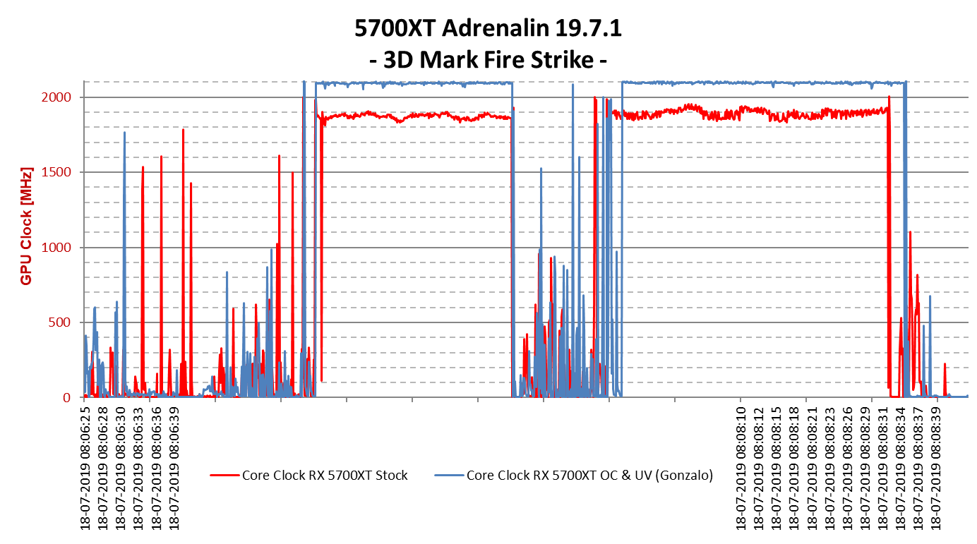
Avg. 1880Mhz.

The point is...

1. RDNA doesn't sustain 2100Mhz... the clocks drops a lot só the card is not running at 36CUs @ 2100Mhz..: that means it is not running anywhere close to 9.9TFs.

2. RDNA performance doesn't scale proportional to clock speeds... at 2100Mhz the performance is not optional proportional to the increase in clock because you are near the limit of the RDNA clocks.

So to avoid both issues that are not present in RDNA 2 you make the test using lower clocks.

Eg.

36 CUs @ 1800Mhz vs 40 CUs @ 1620Mhz
36 CUs @ 1500Mhz vs 40 CUs @ 1350Mhz

In both cases the 36CUs part will delivery better performance.

That is why the test at 2100Mhz is misleading and can't be used as evidence for RDNA 2 high clocks that doesn't suffer in sustain it and it scale better the performance with increase of the clocks over 2000Mhz.
 
Last edited:
Im just joking about the drop features. Hopefully im right it's the full rDNA2... Sony couldn't drop the ball that bad.

But some of you are over selling Mark Sony customisation. Look at the 4 and 4p, still constrain by amd by tsmc or whoever will produce PS5 7nm apu.

I doubt Mark went into PS5 development with the goal to clock up like never before. When it smells like a last minute oc for pr purposes.

Hell, unlike pc, most PS5 users cant even tell what clocks it eventually runs at. Not a case of nvidia 970 when modders ran some script to confirm 970 crippled design and dealing Nvidia a lawsuit and an apology from Jennsung.
All PC cards actually runs at variable clocks... you can't tell it clocks it is running too just like PS5.

The 970 crippled design is related to memory and not clocks.... 0.5GB of the VRAM uses a "half bus" compared with the other 3.5GB due how the modules setup.
 
Last edited:
All PC cards actually runs at variable clocks... you can't tell it clocks it is running too just like PS5.
The 970 crippled design is related to memory and not clocks.... 0.5GB of the VRAM uses a half bus compared with the other 3.5GB.
You can make current pc gpu runs at a narrow sustainable range, as long you apply the right cooling and comfortable volt/freq. I can get my aio cooled 1080ti run at ~1.986ghz in BF1 at 1440p in all maps, verify by msi after burner monitoring.

That's the great thing with pc, you can monitor and test even at end user level. Hence 970 trickery was discovered.

It's hard to know for ps5 case. Even with DF shootout, comparing dynamic res, frame rates and missing graphics is hard to pick up.

Sony can sell PS5 as a 10+ tf machine at $499 and its no problem. Just 15% slower than Series X.

I don't like what Google done with Pixels pricing and i won't accept if Sony goes this route
 
AMD-Wafer-Price-640x362.png

new tech also has a cost (at least at first)
That graph is from 2017, and it might as well be from Stone Age for all the insight it can give today which is none. You see initial costs are always high as R&D is figured into it, and as soon as that node becomes de facto fab, it follows the linear increase in the graph in the long run. So when 6nm or 5nm comes around, 7nm will also be just like one of those points before it, like 20nm.
 
Last edited:
That graph is from 2017, and it might as well be from Stone Age for all the insight it can give today which is none. You see initial costs are always high as R&D is figured into it, and as soon as that node becomes de facto fab, it follows the linear increase in the graph in the long run. So when 6nm or 5nm comes around, 7nm will also just like one of those points before it like 20nm.
If I'm not remembering wrong TSMC said some time ago that 7nm are already cheaper than 16nm.

Edit - I remembered wrong... it is the cost per transistor that is cheaper.... a similar die size in 7nm still cost more than 16nm... the wafer is more expensive (around $10k).
 
Last edited:
What that even means?

Smaller die = more chip per wafer.
So even if the defect rate is the same you still has way more good chips... and cheaper.

But most cases big dies have more defectives because it take a bigger area in the wafer.

Get aggressive with the clocks and the smaller chip could have more defectives. Time will tell how conducive RDNA2 is to a 2.2 clock. In the case of the 5700XT, only about 20% of the dies could support the clocks and power consumption targets of that design (hence enough rejects for 3 consumer products). Now that chip required all CUs to work, so that was another issue.
 
Could Ps5 be having and using the 36 cu without disabling any of them? Wouldn't it be something like 36 cu and 2/4 disabled?
 
AMD-Wafer-Price-640x362.png

new tech also has a cost (at least at first)

With EUV being partially used "most likely" for RDNA2, giving that 50 % efficiency over RDNA 1....that is not free.....

That normalised cost will go up again from RDNA1 to RDNA2 that posters are not budgeting for, We have NO PRICES of RDNA2 yet..

I think these RDNA2 APU's are more expensive than even analysists are budgeting for....dont think we are getting $ 399 consoles.
 
Last edited:
With EU being partially used most likely for some of the RDNA2, that normalised cost will go up again from RDNA1.

I think these RDNA2 APU's are more expensive than even analysists are budgeting for....dont thinkw eare getting $ 399 consoles.
i totally agrre and this is what i was suggesting with this.
 
With EUV being partially used "most likely" for RDNA2, giving that 50 % efficiency over RDNA 1....that is not free.....

That normalised cost will go up again from RDNA1 to RDNA2 that posters are not budgeting for, We have NO PRICES of RDNA2 yet..

I think these RDNA2 APU's are more expensive than even analysists are budgeting for....dont think we are getting $ 399 consoles.

Well, that graph makes a point about smaller chips running at higher clocks ;).
 
Get aggressive with the clocks and the smaller chip could have more defectives. Time will tell how conducive RDNA2 is to a 2.2 clock. In the case of the 5700XT, only about 20% of the dies could support the clocks and power consumption targets of that design (hence enough rejects for 3 consumer products). Now that chip required all CUs to work, so that was another issue.

Key word is "could" as you said and PS5 is likely going for a 40 CU's design with 4 disabled (two DCE's I would guess, not 4 CU's at random).
 
Well, that graph makes a point about smaller chips running at higher clocks ;).

Graph is what is says, Its cost per yielded mm of silicon die vs node size and its clear. People may want to infer frequency or size affects, but that is not what is drawn.

and 7nm+ or P or whatever the marketing term is for RDNA2 is not plotted yet, and our point is at 50 % extra watt efficiency it will be higher.......By an UNKNOWN amount.

Yes I would, but you wouldn't be able to follow. Also, having a good sense of humor would be a must.

I work in semiconductor physics, give me a laugh....
 
Last edited:
Avg. 1880Mhz.

The point is...

1. RDNA doesn't sustain 2100Mhz... the clocks drops a lot só the card is not running at 36CUs @ 2100Mhz..: that means it is not running anywhere close to 9.9TFs.

2. RDNA performance doesn't scale proportional to clock speeds... at 2100Mhz the performance is not optional proportional to the increase in clock because you are near the limit of the RDNA clocks.

So to avoid both issues that are not present in RDNA 2 you make the test using lower clocks.

Eg.

36 CUs @ 1800Mhz vs 40 CUs @ 1620Mhz
36 CUs @ 1500Mhz vs 40 CUs @ 1350Mhz

In both cases the 36CUs part will delivery better performance.

That is why the test at 2100Mhz is misleading and can't be used as evidence for RDNA 2 high clocks that doesn't suffer in sustain it and it scale better the performance with increase of the clocks over 2000Mhz.
My point is RDNA 1 laid the foundation for RDNA 2's higher clock speed when you combine AMD's 50% perf/watt claim.

From
5700xtoc51j1m.png


from https://www.tomshardware.com/news/amd-radeon-5700-xt-overclocked,39916.html
Igor Wallossek, the editor-in-chief of our German-based counterpart, Tom's Hardware Germany, went about outfitting the 5700 XT with a liquid cooler and found that the Navi-based RX 5700 XT is actually quite an impressive overclocking GPU.

Using the powerplay tables method of overclocking AMD GPUs, Wallossek was able to get a 5700 XT to boost to 2.2 GHz, though it averaged a clock speed slightly lower than that. Still, it's an impressive result considering the 5700 XT only averages a clock speed slightly above 2 GHz, with drops well below that threshold at times.


...

You might be thinking the 5700 XT is under liquid cooling because it has to be, or it would thermal throttle, but this overclock didn't really push the 5700 XT very hard. This ~10% overclock only required ~15% more power, which is a far cry from the massive power draw required to push previous Vega-based GPUs (even including the Radeon VII that's based on the same 7nm process). For an overclock of this caliber, you hardly need a liquid cooler, just a decent aftermarket air cooler.


Wallossek's testing bodes very well for future RDNA GPUs and other Navi-based GPUs coming sooner, seeing as the 5700 XT overclocks well without needing very much additional power. Overclockers may consider waiting for custom cards to arrive from AMD's partners, or consider picking up a cheaper air cooler for their GPU from companies like Arctic


------------------------
The foundation for RDNA 2's higher clock speed is found in RDNA 1 and AMD refined it with "50% perf/watt" improvements.


2. Digital Foundry tested 9.67 TFLOPS for both RX 5700 and RX 5700 XT

Your "So to avoid both issues that are not present in RDNA 2 you make the test using lower clocks." argument is without proof.
 
Last edited:
My point is RDNA 1 laid the foundation for RDNA 2's higher clock speed when you combine AMD's 50% perf/watt claim.

From


Your "So to avoid both issues that are not present in RDNA 2 you make the test using lower clocks." argument is without proof.

Yes, and so is your argument without proof ALSO....that RDNA1 scales well to those higher frequencies .....and this data applies to RDNA2 directly.

For RDNA2 we dont know do we, all we know so far is the below from AMD, and what Sony and MS have chosen for their clocks wrt die sizes after extensive modelling / engineering and testing......

If you apply the AMD stated (not claimed as its a statement to investors so legal) 50 % perf per watt to 5700 where do you get to...?

Remember Cerny said there was little advantage going over 2,23 Ghz clock for their APU as they hit other performance restrictions, I wonder what those performance restrictions are for RDNA1 and at what frequency.....?


gkMr45K.png


Remember, Microsoft and Sony engineers are not radid fanboys, they are engineers and will select frequency for the technology based on lots and lots of data on RDNA2 and how it performs not for some number for console wars.
 
Last edited:
Yes, and so is your argument without proof ALSO....that RDNA1 scales well to those higher frequencies .....and this data applies to RDNA2 directly.

For RDNA2 we dont know do we, all we know so far is the below from AMD, and what Sony and MS have chosen for their clocks wrt die sizes after extensive modelling / engineering and testing......

If you apply the AMD stated (not claimed as its a statement to investors so legal) 50 % perf per watt to 5700 where do you get to...?

Remember Cerny said there was little advantage going over 2,23 Ghz clock for their APU as they hit other performance restrictions, I wonder what those performance restrictions are for RDNA1 and at what frequency.....?


gkMr45K.png


Remember, Microsoft and Sony engineers are not radid fanboys, they are engineers and will select frequency for the technology based on lots and lots of data on RDNA2 and how it performs not for some number for console wars.
The argument "So to avoid both issues that are not present in RDNA 2 you make the test using lower clocks" is without proof. Where does it come from?

Non-reference RX 5700 XT factory overclocks at near 2Ghz has 266 to 275 watts average power consumption. Apply AMD's 50% perf/watt improvement claim and it lands around 137.5‬ watts.

APU has extra power consumption from CPU e.g. 35 to 45 watts like mobile Ryzen 7 4800H/HS.

Total power consumption with CPU's 35 watts and GPU's 137.5 watts is around 172.5‬ watts which is similar to X1X's cooling range which is beyond PS4's and PS4 Pro's cooling solution capability.

Sony added another ~230 Mhz on top of 2Ghz for the GPU. Sony's 2230 Mhz for the GPU claim is reachable. Fat PS3's power consumption is around 180 to 201 watts.
 
Last edited:
A quote from the article:

"Several developers speaking to Digital Foundry have stated that their current PS5 work sees them throttling back the CPU in order to ensure a sustained 2.23GHz clock on the graphics core. It makes perfect sense as most game engines right now are architected with the low performance Jaguar in mind - even a doubling of throughput (ie 60fps vs 30fps) would hardly tax PS5's Zen 2 cores. However, this doesn't sound like a boost solution, but rather performance profiles similar to what we've seen on Nintendo Switch. "Regarding locked profiles, we support those on our dev kits, it can be helpful not to have variable clocks when optimising. Released PS5 games always get boosted frequencies so that they can take advantage of the additional power," explains Cerny."

throttling back the CPU to ENSURE GPU sustained clock.

Oh god, there's no one more blind than the person that refuses to see. A quote fro your own quote:

Released PS5 games always get boosted frequencies so that they can take advantage of the additional power," explains Cerny.
 
That comparison is very very misleading.


Because it doesn't fit your preferred narrative? But you are correct, 36 CU vs 40 is not really an accurate comparison of what to expect, they should've used 36 vs 52 in addition to a 2 TF increase on top of it :messenger_tears_of_joy:
 
Last edited:
The argument "So to avoid both issues that are not present in RDNA 2 you make the test using lower clocks" is without proof. Where does it come from?

Non-reference RX 5700 XT factory overclocks at near 2Ghz has 266 to 275 watts average power consumption. Apply AMD's 50% perf/watt improvement claim and it lands around 137.5‬ watts.

APU has extra power consumption from CPU e.g. 35 to 45 watts like mobile Ryzen 7 4800H/HS.

Total power consumption with CPU's 35 watts and GPU's 137.5 watts is around 172.5‬ watts which is similar to X1X's cooling range which is beyond PS4's and PS4 Pro's cooling solution capability.

Sony added another ~230 Mhz on top of 2Ghz for the GPU. Sony's 2230 Mhz for the GPU claim is reachable. Fat PS3's power consumption is around 180 to 201 watts.

Your concern trolling is very interesting using a different RDNA1 and frequencies well about stock is for what exactly - do you actually think we believe that will apply to RDNA2 and Sony and Cerny are numbskulls and Ps5 will perform like a 36 CU at 1.8 Ghz and what Cerny said was crap ?

Nobody is going to decide oh I wont buy a Ps5, because a troller tells us RDNA2 will not be performant at those frequencies......

Give the concern trolling a rest - its called FUD.

Or are you just bored ?
 
With EUV being partially used "most likely" for RDNA2, giving that 50 % efficiency over RDNA 1....that is not free.....

That normalised cost will go up again from RDNA1 to RDNA2 that posters are not budgeting for, We have NO PRICES of RDNA2 yet..

I think these RDNA2 APU's are more expensive than even analysists are budgeting for....dont think we are getting $ 399 consoles.
Well I'm expecting a BOM around $180 for a 360mm2 RDNA 2 chip (the Xbox chip).
How much the PS5 chip BOM will be depend of it size... around 300mm2 probably $120-130.
 
Last edited:
All PC cards actually runs at variable clocks... you can't tell it clocks it is running too just like PS5.

The 970 crippled design is related to memory and not clocks.... 0.5GB of the VRAM uses a "half bus" compared with the other 3.5GB due how the modules setup.
I use MSI Afterburner or FPS Monitor for frame rate, temps, usage load percentage and clock speed graph.
 
Well I'm expecting a BOM around $180 for a 360mm2 RDNA 2 chip (the Xbox chip).
How much the PS5 chip BOM will be depend of it size... around 300mm2 probably $120-130.

I think it will be more than that if TSMC has partially used EUV to get those RDNA2 per / watt benefits, EUV is an astronomical price from ASML and dont you think AMD will want profit and TSMC will want some payback for that 50 % perf / watt gain and massive invetment ?

If Lockart is announced then hold onto your wallets...
 
Last edited:
Your concern trolling is very interesting using a different RDNA1 and frequencies well about stock is for what exactly - do you actually think we believe that will apply to RDNA2 and Sony and Cerny are numbskulls and Ps5 will perform like a 36 CU at 1.8 Ghz and what Cerny said was crap ?

Nobody is going to decide oh I wont buy a Ps5, because a troller tells us RDNA2 will not be performant at those frequencies......

Give the concern trolling a rest - its called FUD.

Or are you just bored ?
You're a hypocrite to label another poster a troll when I stated "Sony's 2230 Mhz for the GPU claim is reachable " i.e I'm supporting Mark Cerny's 2230 Mhz GPU claim.

Read carefully next time.
 
Avg. 1880Mhz.

The point is...

1. RDNA doesn't sustain 2100Mhz... the clocks drops a lot só the card is not running at 36CUs @ 2100Mhz..: that means it is not running anywhere close to 9.9TFs.

2. RDNA performance doesn't scale proportional to clock speeds... at 2100Mhz the performance is not optional proportional to the increase in clock because you are near the limit of the RDNA clocks.

So to avoid both issues that are not present in RDNA 2 you make the test using lower clocks.

Eg.

36 CUs @ 1800Mhz vs 40 CUs @ 1620Mhz
36 CUs @ 1500Mhz vs 40 CUs @ 1350Mhz

In both cases the 36CUs part will delivery better performance.

That is why the test at 2100Mhz is misleading and can't be used as evidence for RDNA 2 high clocks that doesn't suffer in sustain it and it scale better the performance with increase of the clocks over 2000Mhz.
https://www.techpowerup.com/review/amd-radeon-rx-5700-xt/34.html
3649573-8470012438-clock.jpg


Reference RX 5700 XT (40 CU) has 1887 Mhz average clock speed with 9.66 TFLOPS.


https://www.techpowerup.com/review/sapphire-radeon-rx-5700-xt-nitro/33.html

Sapphire Radeon RX 5700 XT Nitro+ already delivers 1971 Mhz average "out-of-the-box" which is 10.09 TFLOPS at 266 watts gaming average.

---

https://www.techpowerup.com/review/msi-radeon-rx-5700-xt-gaming-x/33.html

MSI Radeon RX 5700 XT Gaming X already delivers 1987 Mhz average "out-of-the-box" which is 10,173 TFLOPS at 270 watts gaming average.

---

https://www.techpowerup.com/review/asrock-radeon-rx-5700-xt-taichi-oc-plus/33.html

ASRock Radeon RX 5700 XT Taichi OC+ already delivers 1996 Mhz average "out-of-the-box" which is 10.22 TFLOPS at 274 watts gaming average.

Sony will need RDNA 2's 50% perf/watt improvement.


Try again.
I think you don't read my comments or can't understand.
The RDNA doesn't scale proportionally over 1800-1900Mhz in both power draw and performance

These tests are very misleading... or Apple to oranges.

Show me a RDNA 2 result or a RDNA result where the clock is not near the limit of the RDNA.

Eg.

36 CUs @ 1800Mhz vs 40 CUs @ 1620Mhz
36 CUs @ 1500Mhz vs 40 CUs @ 1350Mhz

That way you won't have the clock not being sustained and you will avoid the disproportional performance and power draw increase.
These are exactly what RDNA 2 differ from RDNA.

PS. For exemple at these high clocks in RDNA the RDNA 2 is probably way over 50% perf. per watt increase because RDNA is near limit and RDNA 2 not.
 
Last edited:
Graph is what is says, Its cost per yielded mm of silicon die vs node size and its clear. People may want to infer frequency or size affects, but that is not what is drawn.

and 7nm+ or P or whatever the marketing term is for RDNA2 is not plotted yet, and our point is at 50 % extra watt efficiency it will be higher.......By an UNKNOWN amount.

Fair enough, won't disagree with you here :).

Improvements in efficiency and maximum clock rate are coming with a cost and it is difficult to think they achieved that much extra efficiency just by architectural improvements and changes to the design/layout. I think the reports by TSMC where a bit moderate in the EUV benefits for 7nm: "TSMC lists its N7+ process as providing a 15% to 20% higher transistor density as well as 10% lower power consumption at the same complexity and frequency".

If the cost per mm2 is rising up at that kind of pace, it does force a good challenge if your design choice requires a bigger and bigger design.

Happy semiconductor professionals are active and contributing to GAF, will be looking forward to your posts :).
That is TSMC talking about N7P to N7+... RDNA is N7.
 
https://www.techpowerup.com/review/amd-radeon-rx-5700-xt/34.html
3649573-8470012438-clock.jpg


Reference RX 5700 XT (40 CU) has 1887 Mhz average clock speed with 9.66 TFLOPS.


https://www.techpowerup.com/review/sapphire-radeon-rx-5700-xt-nitro/33.html

Sapphire Radeon RX 5700 XT Nitro+ already delivers 1971 Mhz average "out-of-the-box" which is 10.09 TFLOPS at 266 watts gaming average.

---

https://www.techpowerup.com/review/msi-radeon-rx-5700-xt-gaming-x/33.html

MSI Radeon RX 5700 XT Gaming X already delivers 1987 Mhz average "out-of-the-box" which is 10,173 TFLOPS at 270 watts gaming average.

---

https://www.techpowerup.com/review/asrock-radeon-rx-5700-xt-taichi-oc-plus/33.html

ASRock Radeon RX 5700 XT Taichi OC+ already delivers 1996 Mhz average "out-of-the-box" which is 10.22 TFLOPS at 274 watts gaming average.

Sony will need RDNA 2's 50% perf/watt improvement.


Try again.
Seems a bad point because done on already selected best chips.
As a console manufacter using this you would want to be lower than this average.
Do we have number with less selection on dies ? the 5700 one. I imagine the average is lower.
 
Last edited:
Fair enough, won't disagree with you here :).

Improvements in efficiency and maximum clock rate are coming with a cost and it is difficult to think they achieved that much extra efficiency just by architectural improvements and changes to the design/layout. I think the reports by TSMC where a bit moderate in the EUV benefits for 7nm: "TSMC lists its N7+ process as providing a 15% to 20% higher transistor density as well as 10% lower power consumption at the same complexity and frequency".

If the cost per mm2 is rising up at that kind of pace, it does force a good challenge if your design choice requires a bigger and bigger design.

Happy semiconductor professionals are active and contributing to GAF, will be looking forward to your posts :).

I am not TSMC level lol.....and Litho is not my area...anyway its fun to speculate and doubt TSMC will give away their secrets anyway.

Your thinking on EUV is all or nothing it seems ? Remember that EUV is just a Litho step before diffusion or etch and Ltho is done many many times as layers and patterns build and all this 7nm+ EUV is marketing.....

From ASML :

DUV Immersion systems can deliver both single-pass and multi-pass lithography and have been designed to be used in combination with EUV lithography to print the different layers of a chip.

So, the APU does not have to be all DUV or all EUV, TSMC can use the prohibitively expensive EUV for critical paths and how much is used and pricing is unknown.

Hence why full EUV is supposed to be full on for 5nm maybe, but EUV probably helped in some gates / fins for 7nm RDNA2 is what I am thinking, Also factor in addition to any design improvements from AMD....hence it will cost more than RDNA1.

If its a little extra cost, then nobody will know as will be lost in Sony and MS end pricing strategy initially, if Ps5 and XSX are $500+ and lockart comes in....mmm. We dont have RDNA prices yet is my point.
 
Last edited:
As i said before, the hint will come from rdna2 gpu. A pity AMD is not launching until late Q3 iirc.
So you don't know then, just making up numbers "normal" clocks and what not
Recycling and disabling, they can work hand on hand. Its seem totally plausible instead of Sony inserting another CU-lite somewhere along the apu
Except they don't... the 4 disabled units have nothing to do with the audio block. Its part of the custom GPU design, a modified CU to more closely resemble a SPU that process audio much more effectively and efficiently "ideal for audio".
Could Ps5 be having and using the 36 cu without disabling any of them? Wouldn't it be something like 36 cu and 2/4 disabled?
Its a 40CU chip with 4 disabled hence 36CUs
The argument "So to avoid both issues that are not present in RDNA 2 you make the test using lower clocks" is without proof. Where does it come from?
5700 hitting diminishing returns at high frequencies because its power starved, the card wasn't designed to clock that high hence why it called an overclock
Game clocks are the sweet spot for that card
 
Last edited:
5700 hitting diminishing returns at high frequencies because its power starved, the card wasn't designed to clock that high hence why it called an overclock
Game clocks are the sweet spot for that card
1. 5700 XT's 40 CU has more SRAM storage when compared to 5700

RxFVwD6.png


Border within the green container refers to CU. Increasing CU count also scales more than just ALUs.

2. Both 5700 and 5700 XT has the same 448 GB/s memory bandwidth. AMD didn't configure higher TFLOPS 5700 XT with higher memory bandwidth.

3. RX 5600 XT OC 36 CU at 7.9 TFLOPS couldn't beat RX 5700 36 CU at 7.7 Ghz due to 336 GB/s vs 448 GB/s memory bandwidth. RX 5600 XT OC at 7.9 TFLOPS has incurred 8% degradation from RX 5700.

4. If RDNA 2 GPU from XSX lands on RTX 2080 level results, I don't see RDNA 2's IPC to be superior to a Turing TU104.

Seems a bad point because done on already selected best chips.
As a console manufacter using this you would want to be lower than this average.
Do we have number with less selection on dies ? the 5700 one. I imagine the average is lower.
That's a yield and maturity issue which is not my argument.

5700 can be re-flashed with RX 5700 XT BIOS and it's a silicon lottery.
 
Last edited:
I think you don't read my comments or can't understand.
The RDNA doesn't scale proportionally over 1800-1900Mhz in both power draw and performance

These tests are very misleading... or Apple to oranges.

Show me a RDNA 2 result or a RDNA result where the clock is not near the limit of the RDNA.

Eg.

36 CUs @ 1800Mhz vs 40 CUs @ 1620Mhz
36 CUs @ 1500Mhz vs 40 CUs @ 1350Mhz

That way you won't have the clock not being sustained and you will avoid the disproportional performance and power draw increase.
These are exactly what RDNA 2 differ from RDNA.

PS. For exemple at these high clocks in RDNA the RDNA 2 is probably way over 50% perf. per watt increase because RDNA is near limit and RDNA 2 not.
Memory bandwidth didn't scale with increase TFLOPS when both RX 5700 and RX 5700 XT has the same 448 GB/s memory bandwidth.

RX 5600 XT 36 CU OC at 7.9 TFLOPS couldn't beat RX 5700 36 CU at 7.7 TFLOPS due to memory bandwidth difference i.e. 336 GB/s vs 448 GB/s respectively.

XSX's memory bandwidth increase matched TFLOPS increase e.g. 25% increase in TFLOPS from RX 5700 XT's 9.6 TFLOPS average with 25% increase in memory bandwidth e.g. 448 GB/s to 560 GB/s

For XSX, MS is throwing higher bus width hardware to deliver RTX 2080 level results shows AMD GPU has inferior tile cache render and/or inferior DCC when compared to RTX 2080 (dedicated 448GB/s VRAM) and RTX 2080 Super (dedicated 496 GB/s VRAM).

RTX 2080 with 448 GB/s + Ryzen 7-3700 with 59GB/s (128 DDR4-3733) has 507 GB/s combined memory bandwidth.

Don't expect miracles from RDNA 2.
 
Last edited:
Graph is what is says, Its cost per yielded mm of silicon die vs node size and its clear. People may want to infer frequency or size affects, but that is not what is drawn.

and 7nm+ or P or whatever the marketing term is for RDNA2 is not plotted yet, and our point is at 50 % extra watt efficiency it will be higher.......By an UNKNOWN amount.


I work in semiconductor physics, give me a laugh....

Well well....good for you. I'm pretty sure you like knock knock jokes...
 
So you don't know then, just making up numbers "normal" clocks and what not

Except they don't... the 4 disabled units have nothing to do with the audio block. Its part of the custom GPU design, a modified CU to more closely resemble a SPU that process audio much more effectively and efficiently "ideal for audio".

Its a 40CU chip with 4 disabled hence 36CUs

5700 hitting diminishing returns at high frequencies because its power starved, the card wasn't designed to clock that high hence why it called an overclock
Game clocks are the sweet spot for that card

As i said, an educated guess from a 20 years console/gaming veteran.

2.23ghz being a 'normal' clocks on the same-ish 7nm process is a stretch. The 5700 ran around ~1.8ghz.
Even if Amd make architecture improvements in rDNA2, this is not reflected in Series X, which will be ~1.85ghz normal.

5700 is not power starved, you can flash the bios and unlocked to give it 300W. The high frequencies limit is just that, limit.
Pushing beyond game 'normal' clocks is just that, overclocking.

PS5 smells awfully like OC.
The best thing, it is hard to prove PS5 games runs at that 10tf most of the time. It is a closed console, unless devs leak out the truths, which they wont since NDA.
So Sony gets away with the PR they wanted.
 
1. 5700 XT's 40 CU has more SRAM storage when compared to 5700

RxFVwD6.png


Border within the green container refers to CU. Increasing CU count also scales more than just ALUs.

2. Both 5700 and 5700 XT has the same 448 GB/s memory bandwidth. AMD didn't configure higher TFLOPS 5700 XT with higher memory bandwidth.

3. RX 5600 XT OC 36 CU at 7.9 TFLOPS couldn't beat RX 5700 36 CU at 7.7 Ghz due to 336 GB/s vs 448 GB/s memory bandwidth. RX 5600 XT OC at 7.9 TFLOPS has incurred 8% degradation from RX 5700.

4. If RDNA 2 GPU from XSX lands on RTX 2080 level results, I don't see RDNA 2's IPC to be superior to a Turing TU104.


That's a yield and maturity issue which is not my argument.

5700 can be re-flashed with RX 5700 XT BIOS and it's a silicon lottery.
1. 2. & 3 why are you even throwing random information with no apparent relation to what i said? Info is great but without context its worthless in a conversation. Try to make a point or concussion
I can understand if English is not your first lenguage, Its not my first language either, but try to improve on this.


Increasing clocks raises the performance of all components not just ALUs
4. I said RDNA2 cards will be designed around higher frequencies, i wasn't talking about IPC that's a topic for another discussion
Current RDNA1 cards reference clockss are much higher compared to GNC but they scale poorly with overclock past this sweet spot the cards are power starved
2.23ghz being a 'normal' clocks on the same-ish 7nm process is a stretch. The 5700 ran around ~1.8ghz.
Even if Amd make architecture improvements in rDNA2, this is not reflected in Series X, which will be ~1.85ghz normal.
We've seen similar breakthroughs on the same node before, which as a 20 years veteran im sure you are aware off
Kepler v1>Kepler v2>Maxwell
Consoles will also use a more refined process

The Xbox chip is bigger so the resulting heat would be much higher than PS5's assuming comparable bins that is why its clocked lower. Smaller chips can reach higher frequencies this is nothing new, seen in CPUs as well
The best thing, it is hard to prove PS5 games runs at that 10tf most of the time. I
We already have Richard claiming they heard from devs running it at a sustained 10.27TF
5700 is not power starved, you can flash the bios and unlocked to give it 300W
Its the board incapable of keeping up with the increased power consumption.
 
Last edited:
1. 2. & 3 why are you even throwing random information with no apparent relation to what i said? Info is great but without context its worthless in a conversation. Try to make a point or concussion
I can understand if English is not your first lenguage, Its not my first language either, but try to improve on this.


Increasing clocks raises the performance of all components not just ALUs
4.
I said RDNA2 cards will be designed around higher frequencies, i wasn't talking about IPC that's a topic for another discussion
Current RDNA1 cards reference clockss are much higher compared to GNC but they scale poorly with overclock past this sweet spot the cards are power starved
This is why I posted the following slide to counter "Increasing clocks raises the performance of all components not just ALUs" argument

3oVFeYA.png

Border within the green container refers to CU. Increasing CU count also scales more than just ALUs.

Increasing GPU clock speed still has memory bandwidth issue and PC's RX 6700 XT SKU may have faster 15000 to 15500 rated GDDR6 memory modules.

PC RDNA 2 SKUs are not limited by the new "budget" GDDR-14000 rated modules e.g. GTX 1660 Super has GDDR6-14000 modules.
 
We've seen similar breakthroughs on the same node before, which as a 20 years veteran im sure you are aware off
Kepler v1>Kepler v2>Maxwell
Consoles will also use a more refined process

The Xbox chip is bigger so the resulting heat would be much higher than PS5's assuming comparable bins that is why its clocked lower. Smaller chips can reach higher frequencies this is nothing new, seen in CPUs as well

We already have Richard claiming they heard from devs running it at a sustained 10.27TF

Its the board incapable of keeping up with the increased power consumption.

Series X and PS5 apu are from same gen.
If Series X comfy clocks is ~1.8ghz, i dont believe PS5 is 2.23ghz.

It is not true smaller chip can reach higher frequencies, at least not 30% higher. My 1080ti can bench comfortably at 2.025ghz, about the same as smaller pascals.

We shall see i guess, at the actual multiplatform games. At best, the frame rates and pixel counting. It is really hard to prove Sony 10tfl claims sadly. Thats what they wanted. :eek:
 
Memory bandwidth didn't scale with increase TFLOPS when both RX 5700 and RX 5700 XT has the same 448 GB/s memory bandwidth.

RX 5600 XT 36 CU OC at 7.9 TFLOPS couldn't beat RX 5700 36 CU at 7.7 TFLOPS due to memory bandwidth difference i.e. 336 GB/s vs 448 GB/s respectively.

XSX's memory bandwidth increase matched TFLOPS increase e.g. 25% increase in TFLOPS from RX 5700 XT's 9.6 TFLOPS average with 25% increase in memory bandwidth e.g. 448 GB/s to 560 GB/s

For XSX, MS is throwing higher bus width hardware to deliver RTX 2080 level results shows AMD GPU has inferior tile cache render and/or inferior DCC when compared to RTX 2080 (dedicated 448GB/s VRAM) and RTX 2080 Super (dedicated 496 GB/s VRAM).

RTX 2080 with 448 GB/s + Ryzen 7-3700 with 59GB/s (128 DDR4-3733) has 507 GB/s combined memory bandwidth.

Don't expect miracles from RDNA 2.
I'm not sure why are replying to me at all.
The comparison is very misleading.
And you reply has nothing to do with what I said.
 
Last edited:
Top Bottom