PS5 Pro devkits arrive at third-party studios, Sony expects Pro specs to leak

Possibly.

Although, PS5-architecture is completely different from PS4 Pro, if I'm not mistaken.
PS4 Pro was nothing but an extra GPU and a bit of extra RAM.

I'm just wondering if these dev kits are actual PS5 Pro devkits, or something in the works for next-gen.
RDNA 1 and RDNA 2 CUs have GCN's Wave64 instruction set backward compatibility. PS5's 36 CU has strict hardware backward compatibility with PS4 Pro's 36 CU and PS4's 18 CU.

RDNA 3 CU has GCN's Wave64 instruction set backward compatibility but dual issue mode is only for Wave32 instruction set. RDNA 3 CU's dual-issue mode is effectively 128 stream processors.
 
Last edited:
NVIDIA reveals Turing RTX, Ampere, and ADA RT TFLOPS vs shader TFLOPS ratio, hence the major reason for AMD's RT is inferior.

xwuc5zm.jpg


According to Microsoft's Xbox Series X, RDNA 2 has shader TFLOPS nearly matching RT TFLOPS i.e. 12 TFLOPS shader with 13 TFLOPS raytracing.

RDNA 3 CU has a 1.5X RT instructions in flight increase.

AMD needs to substantially increase RT's raw TFLOPS performance. AMD needs to treat RT seriously when hardware RT affects professional apps and gaming use cases. Hint: There's NO mobile Radeon RX 7000 series shown on 2024-era laptops during CES 2024.

That RT TFLOP comparison is so superficial that it's almost non-sense.
As it has been stated in several threads, the lacking performance in RT for AMD, is due to several issues.
One is the lack of dedicated units for managing and traversal of the BVH structure. Another is that RT is done in the TMUs.
And probably the worst, is that work wave occupancy with RT loads, is rather low in RDNA2.
FYI, Turing RT cores are next to texture units. https://developer.nvidia.com/blog/nvidia-turing-architecture-in-depth/

BVH data sets are geometry.
 
FYI, Turing RT cores are next to texture units. https://developer.nvidia.com/blog/nvidia-turing-architecture-in-depth/

BVH data sets are geometry.

Being near something does not mean it's the same unit. Turing has dedicated units for ray-tracing. Both for BVH traversal and for for ray and triangle intersection testing.
On RDNA2, the ray and triangle intersection tests are done in the TMUs.

BVH structures are data sets, distributed in a tree. They are not geometry, although they have volumes encompassing geometry.
They can be used to replace geometry in some cases. It's used in Spider-man 2 buildings interiors. In the future we can expect they'll be more and more used instead of geometry.
 
They can be used to replace geometry in some cases. It's used in Spider-man 2 buildings interiors. In the future we can expect they'll be more and more used instead of geometry.

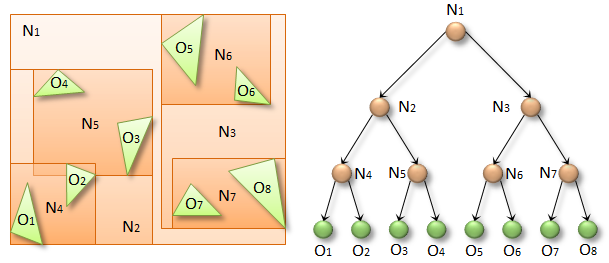
OMG, that is the non-sense from Digital Foundry. A BVH is just a data structure. Something like this.
The BVH encompasses geometry, and divides it in a a data structure, but it's not the geometry.

j4fOBuv.png
 
That RT TFLOP comparison is so superficial that it's almost non-sense.
As it has been stated in several threads, the lacking performance in RT for AMD, is due to several issues.
One is the lack of dedicated units for managing and traversal of the BVH structure. Another is that RT is done in the TMUs.
And probably the worst, is that work wave occupancy with RT loads, is rather low in RDNA2.
Radeon 7900 XTX's 61 TFLOPS shaders,

applying up to 1.5X RT improvement on XSX's 1.08X ratio land on 99 TFLOPS.
applying real-world 1.3X RT improvement on XSX's 1.08X ratio land on 85.9 TFLOPS.

7900 XTX's estimated RT TFLOPS are in the RTX 4070 range.
 
Being near something does not mean it's the same unit. Turing has dedicated units for ray-tracing. Both for BVH traversal and for for ray and triangle intersection testing.
On RDNA2, the ray and triangle intersection tests are done in the TMUs.

BVH structures are data sets, distributed in a tree. They are not geometry, although they have volumes encompassing geometry.
The bound box is an approximation of the geometry mass subset. Ray intersects the triangle test have geometry data.

WyPL7AS.jpg


RDNA 2's RT cores are implemented next to texture units.

On this 7900 XTX's Hog Warts example,

UhiG7KW.jpg


BVH's transversal is a major factor.
 
Last edited:
Radeon 7900 XTX's 61 TFLOPS shaders,

applying up to 1.5X RT improvement on XSX's 1.08X ratio land on 99 TFLOPS.
applying real-world 1.3X RT improvement on XSX's 1.08X ratio land on 85.9 TFLOPS.

7900 XTX's estimated RT TFLOPS are in the RTX 4070 range.

So many problems here.
First, RNDA3 dual compute units are used in pretty much no games so far. And even if it were, it would never be at full peak theoretical ocuppancy.

I don´t know were you got the 1.5X and 1.05x, but the ray and triangle intersection testing is done in the TMUs, not the shaders.
So the scaling has to be done in relation to the amount of TMUs, not the shader or CU count.

AMD and NVidia have different ways of showing their RT numbers. So there is no direct comparison in RT TFLOPs that can be made between the two.
And this is even worse, when we consider that RDNA3 has worse warp/work wave occupancy, than Ada Lovelace.
 
The bound box is an approximation of the geometry mass subset. Ray intersects the triangle test have geometry data.

BVH: Bounding Volume Hierarchy. An "acceleration structure" for ray tracing. Basically a data structure which allows the engine to check quickly what objects a ray (or a bullet) hits.

WyPL7AS.jpg


RDNA 2's RT cores are implemented next to texture units.

Dude, you have the Ray Accelerator right inside the TMU, next to the Texture Filter Units and the Mapping Units.
 
So many problems here.
First, RNDA3 dual compute units are used in pretty much no games so far. And even if it were, it would never be at full peak theoretical ocuppancy.

I don´t know were you got the 1.5X and 1.05x, but the ray and triangle intersection testing is done in the TMUs, not the shaders.
So the scaling has to be done in relation to the amount of TMUs, not the shader or CU count.

AMD and NVidia have different ways of showing their RT numbers. So there is no direct comparison in RT TFLOPs that can be made between the two.
And this is even worse, when we consider that RDNA3 has worse warp/work wave occupancy, than Ada Lovelace.
This is wrong.

gDm8R2R.jpg


S25jEiV.jpg

RDNA 2's ray accelerator unit implementation is next to texture units.

The real issue is I/O bandwidth with the lowest latency SRAM storage.
 
Last edited:
BVH: Bounding Volume Hierarchy. An "acceleration structure" for ray tracing. Basically a data structure which allows the engine to check quickly what objects a ray (or a bullet) hits.


Dude, you have the Ray Accelerator right inside the TMU, next to the Texture Filter Units and the Mapping Units.

Bounding box test example
pSaae5D.jpg


The bound box test is an approximation of the geometry mass subset.
 
This is wrong.

gDm8R2R.jpg


S25jEiV.jpg

RDNA 2's ray accelerator unit implementation is next to texture units.

Here is a deep dive, from an engineer, that explains exactly how RDNA 2 and 3 do RT.


AMD RDNA 2 and RDNA 3

AMD implements raytracing acceleration by adding intersection test instructions to the texture units. Instead of dealing with textures though, these instructions take a box or triangle node in a predefined format. Box nodes can represent four boxes, and triangle nodes can represent four triangles. The instruction computes intersection test results for everything in that node, and hands the results back to the shader. Then, the shader is responsible for traversing the BVH and handing the next node to the texture units. RDNA 3 additionally has specialized LDS instructions to make managing the traversal stack faster.
 
Bounding box test example
pSaae5D.jpg


The bound box test is an approximation of the geometry mass subset.

The bounding volume is just a target volume that encompasses a lot of geometry.
The part that really matters is the hierarchy, as this is the part that will accelerate the Ray Tracing part, by sending the rays to the proper level, so it can hit the correct triangles.
And this is a data structure. Not a geometric structure.

When we talk about acceleration of a BVH, we are talking about data trees:

 
Here is a deep dive, from an engineer, that explains exactly how RDNA 2 and 3 do RT.

LOL. My 7900xtx_hogwarts_indirect_raytracing example is from https://chipsandcheese.com/2023/03/22/raytracing-on-amds-rdna-2-3-and-nvidias-turing-and-pascal

If you read https://chipsandcheese.com/2023/03/22/raytracing-on-amds-rdna-2-3-and-nvidias-turing-and-pascal/

"In the RTX 2060 Mobile's case, L2 latency is around 120 to 143 ns, depending on whether you're going through the TMUs".
 
Last edited:
LOL. My 7900xtx_hogwarts_indirect_raytracing example is from https://chipsandcheese.com/2023/03/22/raytracing-on-amds-rdna-2-3-and-nvidias-turing-and-pascal

If you read https://chipsandcheese.com/2023/03/22/raytracing-on-amds-rdna-2-3-and-nvidias-turing-and-pascal/

"In the RTX 2060 Mobile's case, L2 latency is around 120 to 143 ns, depending on whether you're going through the TMUs".

That is talking about how the data can be shuffled around in the GPU. Because data has to be transferred to different units, as it's operated on.
What that means, is that measuring L2 latency going through the TMU, is higher on Turing. But it does not mean it's the TMU that is doing the ray and triangle testing.

BTW, here is an explanation from the NVidia, about what is a BVH and how to manage it.

 
Last edited:
The bounding volume is just a target volume that encompasses a lot of geometry.
The part that really matters is the hierarchy, as this is the part that will accelerate the Ray Tracing part, by sending the rays to the proper level, so it can hit the correct triangles.
And this is a data structure. Not a geometric structure.

When we talk about acceleration of a BVH, we are talking about data trees:

The BVH tree is a data structure organization and the bound box test is an approximation of the geometry mass subset before drilling down to the ray intersect triangle triangles test.
 
That is talking about how the data can be shuffled around in the GPU. Because data has to be transferred to different units, as it's operated on.
What that means, is that measuring L2 latency going through the TMU, is higher on Turing. But it does not mean it's the TMU that is doing the ray and triangle testing.

BTW, here is an explanation from the NVidia, about what is a BVH and how to manage it.

The priority should be AMD's source, not 3rd party clam chowder.

AMD claims ray accelerators are implemented as separate units next to texture units.
 
The BVH tree is a data structure organization and the bound box test is an approximation of the geometry mass subset before drilling down to the ray intersect triangle triangles test.

The bounding volume is a very coarse entity, that cannot be used to render geometry.
It's only there to set bounds on a group of geometry, to be tested.

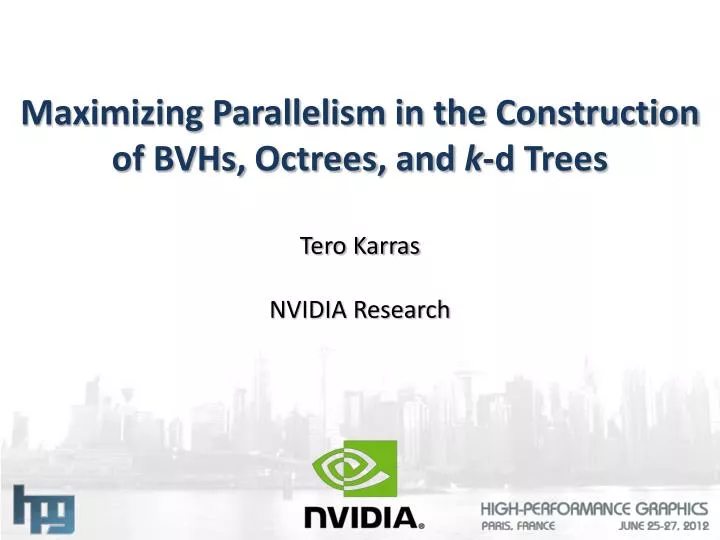
BTW, if you still have doubts that Turing RT cores process the BVH Traversal, and not the TMUs, here is NVidia's presentation:


The RT Cores in Turing can process all the BVH traversal and ray-triangle intersection testing, saving the SM from spending the thousands of instruction slots per ray, which could be an enormous amount of instructions for an entire scene. The RT Core includes two specialized units. The first unit does bounding box tests, and the second unit does ray-triangle intersection tests. The SM only has to launch a ray probe, and the RT core does the BVH traversal and ray-triangle tests, and return a hit or no hit to the SM. The SM is largely freed up to do other graphics or compute work. See Figure 18 or an illustration of Turing ray tracing with RT Cores.
 
That is talking about how the data can be shuffled around in the GPU. Because data has to be transferred to different units, as it's operated on.
What that means, is that measuring L2 latency going through the TMU, is higher on Turing. But it does not mean it's the TMU that is doing the ray and triangle testing.

BTW, here is an explanation from the NVidia, about what is a BVH and how to manage it.

From https://i0.wp.com/chipsandcheese.com/wp-content/uploads/2023/02/rdna2.drawio-1.png?ssl=1

This is from clam chowder

4YugkzA.png

Notice both clam chowder's Ampere and RDNA 2 have "TMU / RT" box.
 
The priority should be AMD's source, not 3rd party clam chowder.

AMD claims ray accelerators are implemented as separate units next to texture units.

AMD shows the Ray-Accelerator inside the TMU.

And here is AMD's patent for using RT in the Texture Units:

 
You have NVidia clearly stating that both the ray and triangle testing and BVH traversal are done in a dedicated RT core, and yet you claim that NVidia is wrong.
While at the same time, for some reason you claim that AMD's RT is not done in the TMUs....
You linked clam chowder's web page before my post when I knew AMD's actual RDNA 2 presentation claims otherwise i.e. AMD added "ray accelerator" units for RDNA 2.

Additional TMUs can be added and why not extra modified TMUs known as ray accelerator units?

ALU SP and TMU ratio has changed in the past Radeon HD series.
 
Last edited:
You linked clam chowder's web page before my post when I knew AMD's actual RDNA 2 presentation claims otherwise i.e. AMD added "ray accelerator" units for RDNA 2.

Additional TMUs can be added and why not extra modified TMUs known as ray accelerator units?

ALU SP and TMU ratio has changed in the past Radeon HD series.

My point is, the Ray Accelerators are in the TMUs both for RDNA2 and RDNA3.
And in Turing, Ampere and Ada, they are in a dedicated RT unit.

Here is RDNA3 ISA, where one might notice that there are a lot of RT instructions, in the section "10.9.3. Texture Resource Definition"
Which is a part of 10.9. "Ray Tracing"

 
AMD shows the Ray-Accelerator inside the TMU.

And here is AMD's patent for using RT in the Texture Units:

That's meaningless when AMD's actual RDNA 2 presentation has additional "ray accelerators" units. AMD has changed stream processors vs TMU ratios in the past Radeon HD series.

The reason why I didn't post Clamchowder's web link is due to conflicts with AMD's official RDNA 2 presentation.
 
My point is, the Ray Accelerators are in the TMUs both for RDNA2 and RDNA3.
And in Turing, Ampere and Ada, they are in a dedicated RT unit.

Here is RDNA3 ISA, where one might notice that there are a lot of RT instructions, in the section "10.9.3. Texture Resource Definition"
Which is a part of 10.9. "Ray Tracing"

Are you claiming CU's TMU vs stream processor ratios never change?
 
That's meaningless when AMD's actual RDNA 2 presentation has additional "ray accelerators" units. AMD has changed stream processors vs TMU ratios in the past Radeon HD series.

The reason why I didn't post Clamchowder's web link is due to conflicts with AMD's official RDNA 2 presentation.

WTF, you have the deep ISA instruction manual, published by AMD, saying it's using Texture Resources, yet you still insist the Ray Accelerators are not in the TMUS.
There is no more concrete evidence, that AMD, themselves, saying it. And they say this both for the RDNA2 ISA and the RDNA3 ISA.
 
WTF, you have the deep ISA instruction manual, published by AMD, saying it's using Texture Resources, yet you still insist the Ray Accelerators are not in the TMUS.
There is no more concrete evidence, that AMD, themselves, saying it. And they say this both for the RDNA2 ISA and the RDNA3 ISA.
Meaningless. Radeon CU's TMU scaling is not static.

AMD's RDNA 3's CU presentation with distinct ray acceleration blocks. Are you claiming AMD's presentation is untrue?

KCqq7Fs.jpg
 
Last edited:
Meaningless. Radeon CU's TMU scaling is not static.

AMD can scale TMUs, CUs, RA and whatever they want as they please.
The fact remains, that AMD does the ray intersection testing in the TMUs and the BVH on the shaders. While NVidia has full dedicated RT cores to do both.
 
AMD can scale TMUs, CUs, RA and whatever they want as they please.
The fact remains, that AMD does the ray intersection testing in the TMUs and the BVH on the shaders. While NVidia has full dedicated RT cores to do both.
Who's fact? Clam Chowder?

Using RT cores in Blender 3D is an extreme RT use case example and it doesn't budget for real-time RT considerations.
 
Last edited:
They can be used to replace geometry in some cases. It's used in Spider-man 2 buildings interiors. In the future we can expect they'll be more and more used instead of geometry.

OMG, that is the non-sense from Digital Foundry. A BVH is just a data structure. Something like this.
The BVH encompasses geometry, and divides it in a a data structure, but it's not the geometry.

j4fOBuv.png
Digital Foundry were correct that RT generates the rooms in the buildings, but it's achieved by a bit of digital trickery. Rooms have been created under the city and based on the ID of the window hit by rays a interior room is then reflected back out. So the geometry still has to be manually created somewhere else but it can be displayed onscreen due to the really clever use use of RT. Starting at 2:47:

 
Digital Foundry were correct that RT generates the rooms in the buildings, but it's achieved by a bit of digital trickery. Rooms have been created under the city and based on the ID of the window hit by rays a interior room is then reflected back out. So the geometry still has to be manually created somewhere else but it can be displayed onscreen due to the really clever use use of RT. Starting at 2:47:


That is not the point I was making, but that the BVH is a data structure. Not geometry.
What is being reflected with RT is normal generated geometry.
The BVH is just the data set that accelerates ray tracing, by defining where rays are cast.
 
That is not the point I was making, but that the BVH is a data structure. Not geometry.
What is being reflected with RT is normal generated geometry.
The BVH is just the data set that accelerates ray tracing, by defining where rays are cast.
Just clearing up the misconception regarding the Spider-Man thing. The building interiors were done by RT but it cannot replace geometry as it was just a bit of clever trickery.
 
Just clearing up the misconception regarding the Spider-Man thing. The building interiors were done by RT but it cannot replace geometry as it was just a bit of clever trickery.

I understand that.
But we have to clarify that DF is constantly making the mistaking of saying that the BVH is geometry, when it's a data structure.
The Bounding Volume is closer in concept to a voxel. Not to geometry with primitives.
 
Last edited:
AMD shows the Ray-Accelerator inside the TMU.

And here is AMD's patent for using RT in the Texture Units:


That's AMD's original 2019 patent.


AMD's US20200193685 is the recent patent that came out in June 2020.
 
When actual specs get leaked if no one else does I am making a new thread because I rarely look in here for a meaningful bump
Did you hear anything about Volume Rendering for Next-Gen?

It's time for true 3D or 4D if they can work melting ice & plant growth into gameplay somehow

( They're not going to stop arguing about Ray tracing are they? Lol)
 
Top Bottom