No, sorry. I once found an old site that had very in-depth comparisons between the three systems (all first generation), including things like die sizes, processes and power consumption. And I believe the Gamecube had a TDP of around 30W, PS2 slightly above 70W and Xbox around 100W, but it's been a while.Do you have a source for that?
I can't seem to find decent looking comparisons on the net anymore. Best I found was this which states 23 W for Gamecube and 32 W for PS2, but it's possible that they used a "fat" PS2's which already had a lower power consumption than the first revisions. I don't remember reading anywhere that PS2 was ever > 46 W though.
-
Hey Guest. Check out your NeoGAF Wrapped 2025 results here!
You are using an out of date browser. It may not display this or other websites correctly.
You should upgrade or use an alternative browser.
You should upgrade or use an alternative browser.
WiiU "Latte" GPU Die Photo - GPU Feature Set And Power Analysis
- Thread starter Thraktor
- Start date
- Status
- Not open for further replies.
lightchris
Member
No, sorry. I once found an old site that had very in-depth comparisons between the three systems (all first generation), including things like die sizes, processes and power consumption. And I believe the Gamecube had a TDP of around 30W, PS2 slightly above 70W and Xbox around 100W, but it's been a while.
That numbers seem like they could be the power supplies' specifications.
JordanN
Banned
I think practically every PS4/XBO game is running at native 1080p which already requires 2.2x more power than 720p so I don't think that's right.So now that we've seen more games from the competition, how does the Latte hold up? I'm starting to think its perhaps a third as powerful as the competition.
Didn't Xbox also have a hard drive? I would take that into account.That numbers seem like they could be the power supplies' specifications.
Doesn't change much, hard disks only consume 5 - 10W.Didn't Xbox also have a hard drive? I would take that into account.
Smurfman256
Member


Graphics look as good as ANY PS4/Xbox one game.
We really haven't seen A) that game in the wild with actual screenshots or B) very many Xbone/PS4 games with similar art styles.
X has some parts which look beyond the 360/ps3, things like lighting,polycount and some higer res textures, but there are also pats which just look like a good looking 360/ps3 game.
and it does not look as good as a PS4/X1 game, they are a step up in lighting, effects, resolution and polycount.
I just watched the trailer where those gifs are from and it does look very impressive.
The fact the games like call of duty ghosts having a separate build for the wiiu/360/ps3 version and the X1/PS4/PC is telling of the WiiU's graphical situation. its seems to be destined to be clump with 360/ps3 ports and get the odd 360+ looking game.
What are you referring to here? Could you give me a link regarding the different versions of Call of Duty: Ghosts please?
We really haven't seen A) that game in the wild with actual screenshots or B) very many Xbone/PS4 games with similar art styles.
What PS4/XBoxOne games have we "seen in the wild"? I certainly don't think WiiU is as powerful, but using the whole "bullshot" argument is quite rich considering what we've seen for PS4 and XBoxOne so far.
What are you referring to here? Could you give me a link regarding the different versions of Call of Duty: Ghosts please?
Would be interesting since they already said the WiiU is using the new engine for COD. They also stated One/PS4 is inferior to the PC version visually. We are basically just seeing your standard pc situation where depending on power under hood settings adjusted accordingly
OG_Original Gamer
Member
Question for the knowledgeable, What would you think of the combination of high speed bandwidth (256) and really fast shader cores, but GPU core clock of 550Mhz?
GameGuru59
Banned
Honestly, FF15 looks sort of like X, and I really don't think it looks that much better to be honest. And that's if those demos were running on actual hardware. And FF15 isn't likely to have as large an open world as X, if it has one at all.What PS4/XBoxOne games have we "seen in the wild"? I certainly don't think WiiU is as powerful, but using the whole "bullshot" argument is quite rich considering what we've seen for PS4 and XBoxOne so far.
Zoramon089
Banned
This is what i am getting at, it is now becoming ingrained that the WiiU will be put in with the X360/PS3.
If the hardware in the WiiU is so good dev's would be making games but they are not, it could be that the WiiU is hard to develop for, but with the low sales it is not really worth investing the time & money in pushing for a release on the WiiU.
Ehh, the hardware probably doesn't have much to do with it, as it's missing out on a bunch of current gen and cross gen titles. And, there are some games like Watch Dogs where the Wii U version is different from the PS3/360 version (it's a PC downport, like the PS4/Xbone are). The same with the recent NFS game. It's on a game by game and dev by dev basis
chaosblade
Unconfirmed Member
Honestly, FF15 looks sort of like X, and I really don't think it looks that much better to be honest. And that's if those demos were running on actual hardware. And FF15 isn't likely to have as large an open world as X, if it has one at all.
It does, unless the game's world design changed (again). Nomura went on the record a couple years ago talking about how big and explorable it was going to be, and we saw a little of it in some of the older trailers. Sounded like it would be akin to Xenoblade on PS3.
I agree that the real-time stuff (not the "target footage" shown during Sony's conference) didn't look THAT much better than X though, but it was also largely unfinished. One scene didn't even water in place around the town yet.
Smurfman256
Member
What PS4/XBoxOne games have we "seen in the wild"? I certainly don't think WiiU is as powerful, but using the whole "bullshot" argument is quite rich considering what we've seen for PS4 and XBoxOne so far.
I meant we haven't seen any screenshots of "X" in the wild or any demos.
GameGuru59
Banned
It does, unless the game's world design changed (again). Nomura went on the record a couple years ago talking about how big and explorable it was going to be, and we saw a little of it in some of the older trailers. Sounded like it would be akin to Xenoblade on PS3.
I agree that the real-time stuff (not the "target footage" shown during Sony's conference) didn't look THAT much better than X though, but it was also largely unfinished. One scene didn't even water in place around the town yet.
Yeah... I wouldn't count on that open world. Looking at them again, none of the recent trailers highlight anything to that effect. We'll see though. Right now, 15 looks like a 3 way cross between Darksiders, Bayonetta, and FF12. The one thing I do like in the game is the physics. Objects seem to have a good weight to them, environments are somewhat destructable, and I can see clear evidence of tessellation in the water in one scene. Its that stuff that scares me with Wii U. I hope the CPU has enough heft to handle a large amount of physics based stuff.
On the other hand, I see nothing in that demo that the Wii U couldn't run with lower graphical fidelity. The hardware would be only holding back the graphics, not the gameplay as has been true in the past. Diminishing returns are upon us.
lwilliams3
Member
So now that we've seen more games from the competition, how does the Latte hold up? I'm starting to think its perhaps a third as powerful as the competition.
I believe the gap is a bit more than that. The issue with looking at the games from the competition is that they are pre-launch games. Like the Wii U, they will improve in time. Just don't expect them to beat PC. That CoD info involving PC textures really seem to impact some people.
The big question here is: Will the visual gap between the Wii U and XB1/PS4 narrow, widen, or stay the same throughout the generation? There are alot of factors involved with that.
What are you referring to here? Could you give me a link regarding the different versions of Call of Duty: Ghosts please?
Would be interesting since they already said the WiiU is using the new engine for COD. They also stated One/PS4 is inferior to the PC version visually. We are basically just seeing your standard pc situation where depending on power under hood settings adjusted accordingly
Yes, I was wondering about that too.
phosphor112
Banned
Yeah... I wouldn't count on that open world. Looking at them again, none of the recent trailers highlight anything to that effect. We'll see though. Right now, 15 looks like a 3 way cross between Darksiders, Bayonetta, and FF12. The one thing I do like in the game is the physics. Objects seem to have a good weight to them, environments are somewhat destructable, and I can see clear evidence of tessellation in the water in one scene. Its that stuff that scares me with Wii U. I hope the CPU has enough heft to handle a large amount of physics based stuff.
On the other hand, I see nothing in that demo that the Wii U couldn't run with lower graphical fidelity. The hardware would be only holding back the graphics, not the gameplay as has been true in the past. Diminishing returns are upon us.
No, there are plenty of calculations that still can't be done. Even if not part of the graphics pipeline, it'll affect graphics.
Hell, we are going to go through another generation with probably mostly baked lighting.
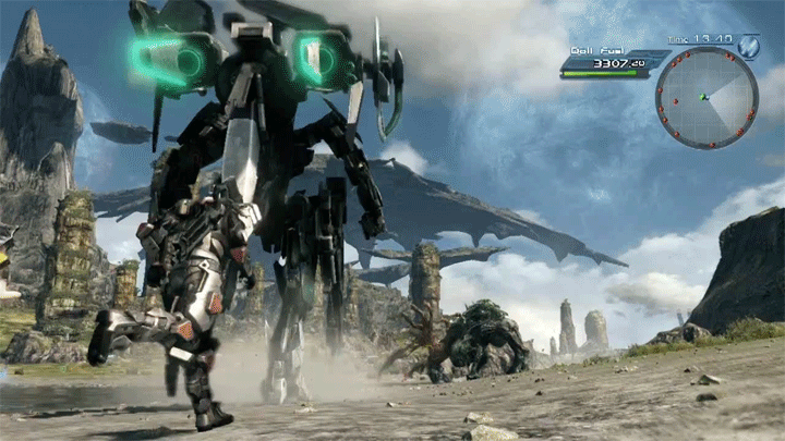
Man, those X gifs are so annoying.
It's a nice game but it's also barren. PS4/XBO at least have games that are both impressive and show more than one character at a time.
Well the shot in the mech hangar does indeed show more than one character (Not exactly sure if you were talking about NPCs or just playable characters). They're also doing different things. The guys to the left are giving each other a high five. You can see two characters to the right conversing while one is drinking from a canister. A character to the front is giving a mech directions and you can see two characters next to him walking by talking to each other. A downsized gif isn't the best way to show this, just watch the trailer instead.
I also don't want to clog up the thread with more gifs. They've been posted enough already.
The shot of him walking through the town also shows more than one NPC. Also remember that this is a game still in development, we have no idea how Monolith plans to fill their open world, but I can already tell the draw distance for monsters is already going to be significantly better than it was on Xenoblade. If you look at the scene with the walking mech transforming into the the vehicle you can see a giant looking bird monster far in the distance.
Also the XB1 and PS4 comparisons need to end now. All they do is ignite console war bullcrap. PS4 and XB1 have better specs, end of discussion. But I still think Wii U will have very nice looking games. Looking forward to seeing what else Nintendo can pull off in the future with this hardware.
JordanN
Banned
The "one character" was kind of a tongue in cheek, since obviously there were 2 or 3 people accompanying the player. The point however was, someone was comparing it to PS4/XBO which I saw as sort of insulting when there are games on those platforms that were not only pushing graphics, but also had way more characters and objects on display. Even if Monolith plans to do more, I thought it was an important distinction that needs to be made.Well the shot in the mech hangar does indeed show more than one character (Not exactly sure if you were talking about NPCs or just playable characters). They're also doing different things. The guys to the left are giving each other a high five. You can see two characters to the right conversing while one is drinking from a canister. A character to the front is giving a mech directions and you can see two characters next to him walking by talking to each other. A downsized gif isn't the best way to show this, just watch the trailer instead.I also don't want to clog up the thread with more gifs. They've been posted enough already.
The shot of him walking through the town also shows more than one NPC. Also remember that this is a game still in development, we have no idea how Monolith plans to fill their open world, but I can already tell the draw distance for monsters is already going to be significantly better than it was on Xenoblade. If you look at the scene with the walking mech transforming into the the vehicle you can see a giant looking bird monster far in the distance.
Also the XB1 and PS4 comparisons need to end now. All they do is ignite console war bullcrap. PS4 and XB1 have better specs, end of discussion. But I still think Wii U will have very nice looking games. Looking forward to seeing what else Nintendo can pull off in the future with this hardware.
The "one character" was kind of a tongue in cheek, since obviously there were 2 or 3 people accompanying the player. The point however was, someone was comparing it to PS4/XBO which I saw as sort of insulting when there are games on those platforms that were not only pushing graphics, but also had way more characters and objects on display. Even if Monolith plans to do more, I thought it was an important distinction that needs to be made.
"Insulting"? Lol. Dude, seems you take this stuff way too seriously. I mean it's cool to analyze and stuff and there is a great discussion to be had here, but to use words like "insulting" just kinda seems like your taking this stuff pretty personally. Either that or you see these consoles as living creatures with feelings. lol
Mihael Mello Keehl
Banned
Are you surprised? Lol he said Nintendo was immoral for pikmin 3s graphics lol"Insulting"? Lol. Dude, seems you take this stuff way too seriously. I mean it's cool to analyze and stuff and there is a great discussion to be had here, but to use words like "insulting" just kinda seems like your taking this stuff pretty personally. Either that or you see these consoles as living creatures with feelings. lol
Smurfman256
Member
Are you surprised? Lol he said Nintendo was immoral for pikmin 3s graphics lol
I would like a link to where he said that.
PotionBleue
Member
This might be a stupid question, but has it been confirmed whether the Wii U can read dual-layer Wii U discs (~50 GB instead of 25) or not?
This might be a stupid question, but has it been confirmed whether the Wii U can read dual-layer Wii U discs (~50 GB instead of 25) or not?
I think all the documentation states 25gb. However, with it being a blu ray drive in all but name, I am not sure if that is a technical limitation on it or just the max size that Nintendo currently wants to stamp out of the factories as DL BDs are still more expensive.
Smurfman256
Member
I think all the documentation states 25gb. However, with it being a blu ray drive in all but name, I am not sure if that is a technical limitation on it or just the max size that Nintendo currently wants to stamp out of the factories as DL BDs are still more expensive.
call me kooky, but did Nintendo every say that the Wii could support DL before Brawl?
Mihael Mello Keehl
Banned
It was some pikmin 3 threadI would like a link to where he said that.
GameGuru59
Banned
Well, I meant it in the sense of the traditional way we have of rendering graphics right now (basically faking alot of stuff). Once we get around to doing alot of global illumination and begin to see ray tracing in games, that's where you'll see (the final?) generational leap. That's next, next gen though.No, there are plenty of calculations that still can't be done. Even if not part of the graphics pipeline, it'll affect graphics.
Hell, we are going to go through another generation with probably mostly baked lighting.
chaosblade
Unconfirmed Member
call me kooky, but did Nintendo every say that the Wii could support DL before Brawl?
I don't remember them ever mentioning it, but I could be mistaken.
I'm not sure there would be many games that would require DL-BD anyway. On PS3 most of the games that take advantage of them use it for high quality sound for voice acting in multiple languages and two versions of each pre-rendered cutscene for 2D and 3D versions. Things that you generally aren't going to see that much of on Nintendo's consoles anyway.
foxuzamaki
Doesn't read OPs, especially not his own
I would like a link to where he said that.
I havent seen that exact quote but go into any pikmin 3 thread pre-release, you can see him preaching up and down how bad the graphics are, the only thread i actually havent seen him in is the thread where someone posted saying pikmin 3 looked damn good
Horse Armour
Member
What I don't get about JordanN is that just a few months ago he was one of the biggest Nintendo fanboys on GAF almost rivaling the likes of AceBandage and SnesFreak. He was one of the biggest evangelists of the Wii U's hardware superiority over 360/PS3 which is what caused him to get his tag where he claimed to be able to count the polygons in Wii U games proving that they were far superior to PS3/360 titles. I even remember him trying to convince everyone that NSMBU featured global illumination because it featured a bouncing dynamic light which has been seen in games since the 90s. What happened in these last few months to turn him to the polar opposite?
What I don't get about JordanN is that just a few months ago he was one of the biggest Nintendo fanboys on GAF almost rivaling the likes of AceBandage and SnesFreak. He was one of the biggest evangelists of the Wii U's hardware superiority over 360/PS3 which is what caused him to get his tag where he claimed to be able to count the polygons in Wii U games proving that they were far superior to PS3/360 titles. I even remember him trying to convince everyone that NSMBU featured global illumination because it featured a bouncing dynamic light which has been seen in games since the 90s. What happened in these last few months to turn him to the polar opposite?
Too much time in a single thread about a single thing that gets argued in a circular manner tends to do that. People start to follow that circle themselves.
What I don't get about JordanN is that just a few months ago he was one of the biggest Nintendo fanboys on GAF almost rivaling the likes of AceBandage and SnesFreak. He was one of the biggest evangelists of the Wii U's hardware superiority over 360/PS3 which is what caused him to get his tag where he claimed to be able to count the polygons in Wii U games proving that they were far superior to PS3/360 titles. I even remember him trying to convince everyone that NSMBU featured global illumination because it featured a bouncing dynamic light which has been seen in games since the 90s. What happened in these last few months to turn him to the polar opposite?
He realized Nintendo abandoned him. It was a slow painful process, but it finally hit him 2 months after Wii U's release.
foxuzamaki
Doesn't read OPs, especially not his own
What I don't get about JordanN is that just a few months ago he was one of the biggest Nintendo fanboys on GAF almost rivaling the likes of AceBandage and SnesFreak. He was one of the biggest evangelists of the Wii U's hardware superiority over 360/PS3 which is what caused him to get his tag where he claimed to be able to count the polygons in Wii U games proving that they were far superior to PS3/360 titles. I even remember him trying to convince everyone that NSMBU featured global illumination because it featured a bouncing dynamic light which has been seen in games since the 90s. What happened in these last few months to turn him to the polar opposite?
i didnt have a account back then, was just a lurker, but i remember this aswell though i wouldnt call him a nintendo fanboy
Most people you see actively bashing Nintendo are disgruntled fanboys of old that demand the company evolved according to their tastes and whims.What I don't get about JordanN is that just a few months ago he was one of the biggest Nintendo fanboys on GAF almost rivaling the likes of AceBandage and SnesFreak. He was one of the biggest evangelists of the Wii U's hardware superiority over 360/PS3 which is what caused him to get his tag where he claimed to be able to count the polygons in Wii U games proving that they were far superior to PS3/360 titles. I even remember him trying to convince everyone that NSMBU featured global illumination because it featured a bouncing dynamic light which has been seen in games since the 90s. What happened in these last few months to turn him to the polar opposite?
The_Intruder
Member
. I even remember him trying to convince everyone that NSMBU featured global illumination because it featured a bouncing dynamic light which has been seen in games since the 90s.
Wow! nice one haha! And after Mario kart 8 and X were shown, he was desappointed by the graphics but claims before the superiority of the wiiu with launch port and Nsmbu... I don't understand this guy...
Apophis2036
Banned
i didnt have a account back then, was just a lurker, but i remember this aswell though i wouldnt call him a nintendo fanboy
He was a very vocal supporter of Nintendo and the WiiU though, makes the extreme turnaround pretty strange.
Wasn't he the guy that said he had the choice of a WiiU at launch or a PS3 as he had never owned a PS3 or 360 ?. If so it's kind of obvious what he chose.
With regards to 'baked lighting', I don't know why people care tbh, unless they want a day / night cycle. If baked lighting keeps the framerate around 30fps instead of having it in the low 20's then I hope developers continue using it.
Fourth Storm
Member
I don't really care what Wii U's ALU count is, I only originally cared because I wondered how it stacked up to Xenos, but Xenos was so poor in efficiency that once I dug into it's performance and found that it was almost half as powerful as I thought it was, Wii U's bare minimum spec would be able to clearly win in performance, so I found little reason to care beyond that, but all the people throwing around 160 ALUs only do so because the majority of people following these threads have taken that number as fact, when in reality it is a poor guess based on performance of one game with a small budget not trying to push the console in any real way. I still think it is more likely that 320 ALUs makes sense and one reason fourth storm decided it didn't is because he heard from someone (a rumor) that Latte was actually a 45nm process chip, but I find that very odd since no AMD GPU has ever been 45nm afaik, and even the r700 was produced at 40nm and was found to be significantly more efficient, Nintendo's design does go against using 45nm here and just makes very little sense when the MCM was needed to hit more exact performance than anything Nintendo has made in the past.
Just catching up with this thread. Man oh man, it's getting a bit crazy in here!
Anyway, z0m, I don't think 45nm vs 40nm is that big of a deal as much as I do the switch to a different manufacturer - namely Renesas, who to my knowledge have never manufactured a Radeon part previously. Add to the fact that they had to put the blocks on an eDRAM friendly process and that might also account for less density.
Another thing I learned recently in regards to the Brazos size comparisons is that the ALUs in that design lack double precision floating point capabilities. We don't know if Latte has this or not, but considering the fact that Iwata called it a "GPGPU," we can at least entertain the possibility that it might, as double-precision math is an important aspect of many OpenCL applications. If Latte's shaders do this, it could also contribute to their larger relative size.
No, my biggest reasons for rejecting anything other than 160 shaders at this point are the register banks within the shaders, the TMU count, and the TDP.
On a different note, I actually took to studying the die a bit more last night (I have no idea why it gives me such entertainment) while using Brazos as a reference. One of the things that has bothered me is the V block on Latte. I have, up until now, identified it as the Global Data Share, and pegged it at 64kiB. I didn't find this ID entirely satisfactory, however. The main reason is that to have no sort of memory controller adjacent to the DDR3 interface would be quite unusual. I also found it suspicious that the block housed two symmetric SRAM groups rather than one large pool.
Anyway, when I got to looking at Brazos again, I realized that even though the GPU supposedly has a 64kiB GDS, I couldn't for the life of me locate it. That much memory should be easy to find. I finally concluded that the only place that it could be located is within the Shader Export block. Looking at some GCN documentation (this part of which we can probably apply to previous designs as well), it stated that export is the path to GDS.
So I now believe Latte's GDS to be found within the Shader Export block, namely Block P. I am less confident on the size of the memory store now, but it's probably somewhere between 16kB (as in R700) and 64 kB (as in everything later than R700). It also makes sense that this block is adjacent to the blocks I believe are the Local Data Shares, the Q blocks.
Meanwhile, Block R is probably the North Bridge, as it seems to resemble other NB designs and features some dual ported SRAM, which I figure might be useful in such a block. It's also adjacent to the eDRAM and whatever kindof channel/bus thingy is going on in the middle of it. Block V would then be some type of DMA engine or an additional memory controller for the DDR3 memory, if the NB is meant specifically to handle access to the eDRAM. Maybe something like the separate "MAC" blocks described in the patent for Flipper's "enhanced memory controller." Block O might be a hub designed to arbitrate memory accesses from the UVD, Display Controller, DSP, and other less bandwidth intensive components separate from the graphics pipeline.
Finally, I think the 3 MB MEM 0 is probably being used by Nintendo as a cache of sorts for intercommunication between the CPU and GPU (conveniently the same size as the CPU's L2), and the Front Side Bus hardware is most likely Block A.
Just wanted to chime in and thank namely fourth storm, blu, thraktor, bg and others for theire continuous analasys throughout the wust threads. Have followed them since wust 1 when i was still a non-member to great enjoyment. Also special thanks to burntpork, that guy was amazing ")
Anyway, 160 alus does sound dissapointing, but you obviously know a lot about these things fourth storm and your theories do sound plausible, so I value your analysis.
Now back to lurking")
Anyway, 160 alus does sound dissapointing, but you obviously know a lot about these things fourth storm and your theories do sound plausible, so I value your analysis.
Now back to lurking
Just wanted to chime in and thank namely fourth storm, blu, thraktor, bg and others for theire continuous analasys throughout the wust threads. Have followed them since wust 1 when i was still a non-member to great enjoyment. Also special thanks to burntpork, that guy was amazing
Anyway, 160 alus does sound dissapointing, but you obviously know a lot about these things fourth storm and your theories do sound plausible, so I value your analysis.
Now back to lurking
I had been in each of the WUST threads, so deep down inside I expected more power, but was not surprised at what we got. Its impressive tech for a 33 watt system.
blu
Wants the largest console games publisher to avoid Nintendo's platforms.
Doubles is something quite a few GPGPUs live happily without, and many of those which do support doubles are doing it 'half-heartedly', so I think we can safely drop this line of thinking ; ) Fun fact: NV have been wielding doubles support left and right in their designs, even across the value mobile parts. I'm still not sure why, but that's what they do.Another thing I learned recently in regards to the Brazos size comparisons is that the ALUs in that design lack double precision floating point capabilities. We don't know if Latte has this or not, but considering the fact that Iwata called it a "GPGPU," we can at least entertain the possibility that it might, as double-precision math is an important aspect of many OpenCL applications. If Latte's shaders do this, it could also contribute to their larger relative size.
BTW, I don't recall if I ever mentioned that, but nevertheless, a small detail re AMD's entire Xenos and VLIW-based architecture lineup - their GPRs are all single-ported. It's a trade-off which allows AMD to put larger register files at the expense of some clever register access shuffling.No, my biggest reasons for rejecting anything other than 160 shaders at this point are the register banks within the shaders, the TMU count, and the TDP.
Fourth Storm
Member
Just wanted to chime in and thank namely fourth storm, blu, thraktor, bg and others for theire continuous analasys throughout the wust threads. Have followed them since wust 1 when i was still a non-member to great enjoyment. Also special thanks to burntpork, that guy was amazing
Anyway, 160 alus does sound dissapointing, but you obviously know a lot about these things fourth storm and your theories do sound plausible, so I value your analysis.
Now back to lurking
Always nice to know I'm not just talking to myself! The power of the system is really a moot point now, I think, but trying to ID the different blocks and such is a fun exercise in research and logic.
Doubles is something quite a few GPGPUs live without happily, and many of those who do support doubles are doing it 'half-heartedly', so I think we can safely drop this line of thinking ; ) Fun fact: NV have been wielding doubles support left and right in their designs, even across the value mobile parts. I'm still not sure why, but that's what they do.
BTW, I don't recall if I ever mentioned that, but nevertheless, a small detail re AMD's entire Xenos and VLIW-based architecture lineup - their GPRs are all single-ported. It's a trade-off which allows AMD to put larger register files at the expense of some clever register access shuffling.
Interesting point on the doubles, blu. So it seems unlikely, but I still don't know if I would completely discount the possibility. Nintendo can be random like that. But you're right in implying that we shouldn't base our whole line of thought on the assumption that the ALUs perform double precision.
So dual-ported registers in an AMD card would be highly unusual. I don't know if this was your point, but that seems to support what I've read about GPRs and how the number of individual SRAM banks is indicative of 20 ALUs per block. Marcan also identified the red SRAM blocks as dual-ported. He may have been mistaken, but that's what I've been going with, as he was pretty on point with the other IDs he made.
Finally, I think the 3 MB MEM 0 is probably being used by Nintendo as a cache of sorts for intercommunication between the CPU and GPU (conveniently the same size as the CPU's L2), and the Front Side Bus hardware is most likely Block A.
I was thinking the same thing. The 1MB SRAM bank, especially, may be a giveaway.
Why else would they use that amount if die space for SRAM - when eDRAM would double the capacity for the same area - unless they were specifically aming for the lowest possible latency? Being that all this (already low latency) eDRAM is right there on the GPU, it would only make sense that additional lower latency SRAM would be for 'intense' CPU-GPU communications. I was glad to see Shin'en mentioning this particular interaction as an area that interest them.
I don't think the other 2MB - despite the total being equal to the CPU's L2 - was meant for that kind of interaction. That's not to say it can't be treated that way. I was wondering if it was instead meant to "free up" the bigger eDRAM pool from other bandwidth intensive processes, like transparencies, post FX, or even AA, if coded accordingly. Past Nintendo architecture did kinda split up eDRAM pools for specific graphical tasks, so I could see them employing a similar design philosophy again. What ever the case, all these high bandwidth pools in Wii U is sure to produce valuable techniques, and some impressive results once developers really start tapping into them.
Fourth Storm
Member
I was thinking the same thing. The 1MB SRAM bank, especially, may be a giveaway.
Why else would they use that amount if die space for SRAM - when eDRAM would double the capacity for the same area - unless they were specifically aming for the lowest possible latency? Being that all this (already low latency) eDRAM is right there on the GPU, it would only make sense that additional lower latency SRAM would be for 'intense' CPU-GPU communications. I was glad to see Shin'en mentioning this particular interaction as an area that interest them.
I don't think the other 2MB - despite the total being equal to the CPU's L2 - was meant for that kind of interaction. That's not to say it can't be treated that way. I was wondering if it was instead meant to "free up" the bigger eDRAM pool from other bandwidth intensive processes, like transparencies, post FX, or even AA, if coded accordingly. Past Nintendo architecture did kinda split up eDRAM pools for specific graphical tasks, so I could see them employing a similar design philosophy again. What ever the case, all these high bandwidth pools in Wii U is sure to produce valuable techniques, and some impressive results once developers really start tapping into them.
Yeah, it's hard to tell for sure exactly how MEM0 is utilized, but we have hints in that Marcan told us that it's kernel-level stuff and pretty much off limits to devs, which is why I posited an automated cache sort of thing. That 1 MB of it is SRAM likely has more to do with the way the embedded texture cache in Flipper was split up into 32 macros, each with its own address bus. I believe blu was the first one in these threads to make that point.
blu
Wants the largest console games publisher to avoid Nintendo's platforms.
BTW, just another semantics note: the fact a buffer is off-limits for a user-land host process (i.e CPU user-land code) does not necessary imply the buffer is off-limits for client access, fullstop. The established GPGPU memory models have various pools inaccessible to (user-world) host code, but trivially accessible to GPU user kernels. Case in point, my CPU process may not be able to fetch a single bit off a compute unit's LDS, but my OpenCL GPU kernel can access it all it wants, and, if needed, interface it to my CPU code (i.e. route contents to a buffer accessible to the CPU).Yeah, it's hard to tell for sure exactly how MEM0 is utilized, but we have hints in that Marcan told us that it's kernel-level stuff and pretty much off limits to devs, which is why I posited an automated cache sort of thing. That 1 MB of it is SRAM likely has more to do with the way the embedded texture cache in Flipper was split up into 32 macros, each with its own address bus. I believe blu was the first one in these threads to make that point.
ThaGuy
Member
I would like to thank all the people who been using all of their brain power for this thread. Even though I don't understand alot of the tech jargon, Its still refreshing/scary that we put more time into figuring out what makes the Wii U tick than some developers.
Keep up the good work people.
Keep up the good work people.
Mihael Mello Keehl
Banned
Well its impossible to do that anymore with that tag, no one will take you seriously. Might as well change views on the fly.What I don't get about JordanN is that just a few months ago he was one of the biggest Nintendo fanboys on GAF almost rivaling the likes of AceBandage and SnesFreak. He was one of the biggest evangelists of the Wii U's hardware superiority over 360/PS3 which is what caused him to get his tag where he claimed to be able to count the polygons in Wii U games proving that they were far superior to PS3/360 titles. I even remember him trying to convince everyone that NSMBU featured global illumination because it featured a bouncing dynamic light which has been seen in games since the 90s. What happened in these last few months to turn him to the polar opposite?
lostinblue
Banned
I do believe that focus has something to do with Raytracing capabilities, remember Nvidia is undisputed market leader in the professional segment (FireGL has nothing against Quadro); it's there not for games but for the advent of professional toolset acceleration; and home GPU's are basically laser cut down Quadro's so it all adds up.Doubles is something quite a few GPGPUs live without happily, and many of those who do support doubles are doing it 'half-heartedly', so I think we can safely drop this line of thinking ; ) Fun fact: NV have been wielding doubles support left and right in their designs, even across the value mobile parts. I'm still not sure why, but that's what they do.
I know it's relevant to use double precision for ray tracing, you can use reduced precision on some renderers but it's certainly not preferable. This said I actually don't know much about specifics as I do some modeling but I usually don't read the documentation for it. I reckon I'm right on the money though.
As for going as far as putting it onto their mobile solutions, that's a pretty big question mark; but on regular GPU's I can understand .
Just catching up with this thread. Man oh man, it's getting a bit crazy in here!
Anyway, z0m, I don't think 45nm vs 40nm is that big of a deal as much as I do the switch to a different manufacturer - namely Renesas, who to my knowledge have never manufactured a Radeon part previously. Add to the fact that they had to put the blocks on an eDRAM friendly process and that might also account for less density.
Another thing I learned recently in regards to the Brazos size comparisons is that the ALUs in that design lack double precision floating point capabilities. We don't know if Latte has this or not, but considering the fact that Iwata called it a "GPGPU," we can at least entertain the possibility that it might, as double-precision math is an important aspect of many OpenCL applications. If Latte's shaders do this, it could also contribute to their larger relative size.
No, my biggest reasons for rejecting anything other than 160 shaders at this point are the register banks within the shaders, the TMU count, and the TDP.
Finally, I think the 3 MB MEM 0 is probably being used by Nintendo as a cache of sorts for intercommunication between the CPU and GPU (conveniently the same size as the CPU's L2), and the Front Side Bus hardware is most likely Block A.
Yeah, people got a little carried away while the tech heads were gone.
Brazo actually does do some GPGPU things, in fact a university decided to use this processor and ended up nearly doubling the compute speed of every day use thanks to some home made drivers using the GPU for GPGPU tasks whenever possible.
Not sure Renesas is really going to offer that big of a difference, that is part of the point I'm trying to make, since they are so great at memory modules, is it also possible that the count of the registry is wrong and they are using larger modules there? they have always looked bigger to me compared to the brazo shots. Even if it isn't there is the possibility that the cache doesn't need to be as big thanks to not doing all the things a GPU normally does (mostly in video land here) as well as having all the extra eDRAM and SRAM on chip in other places.
The power consumption is the last thing I would use to attribute to only having 160ALUs, the targeted low clock, mature 40nm process using a low power format as well as it being on a MCM, it could be saving quite a bit of power, every power consumption guess I've seen never takes those things into account.
Mem 0 could be used for a number of things, my guess is that it is being used exactly like Gamecube's texture memory, as the edram should be large enough to cache the cpu pool as needed, leaving the faster latency SRAM for heavy latency GPU specific things. As I mentioned above I also think some of this memory can be used in place of some registry space, such as GPGPU instruction caching, or a number of other tasks that you would want quick access to but doesn't need to be exactly immediate.
Disclaimer: Although I do some light programming, this is a hobby for me and I do not have a computer science degree, nor do I code in OpenCL.
Fourth Storm
Member
BTW, just another semantics note: the fact a buffer is off-limits for a user-land host process (i.e CPU user-land code) does not necessary imply the buffer is off-limits for client access, fullstop. The established GPGPU memory models have various pools inaccessible to (user-world) host code, but trivially accessible to GPU user kernels. Case in point, my CPU process may not be able to fetch a single bit off a compute unit's LDS, but my OpenCL GPU kernel can access it all it wants, and, if needed, interface it to my CPU code (i.e. route contents to a buffer accessible to the CPU).
So basically, the more we think we know, the less we actually do. Btw, you still owe me a story.
Yeah, people got a little carried away while the tech heads were gone.
Brazo actually does do some GPGPU things, in fact a university decided to use this processor and ended up nearly doubling the compute speed of every day use thanks to some home made drivers using the GPU for GPGPU tasks whenever possible.
Not sure Renesas is really going to offer that big of a difference, that is part of the point I'm trying to make, since they are so great at memory modules, is it also possible that the count of the registry is wrong and they are using larger modules there? they have always looked bigger to me compared to the brazo shots. Even if it isn't there is the possibility that the cache doesn't need to be as big thanks to not doing all the things a GPU normally does (mostly in video land here) as well as having all the extra eDRAM and SRAM on chip in other places.
The power consumption is the last thing I would use to attribute to only having 160ALUs, the targeted low clock, mature 40nm process using a low power format as well as it being on a MCM, it could be saving quite a bit of power, every power consumption guess I've seen never takes those things into account.
That's an interesting fact about Brazos. Just goes to show what 80 shaders can do!
On the topic of the fab house, I suppose this is another place where we differ. You don't see it as having much of an impact on component size, and I can see it as potentially having a huge one. Despite the maturity of whatever process (40nm, 45nm...) they used, the fact is that they don't have much experience with Radeon blocks whereas TSMC do. And this is nothing against Renesas. It just doesn't seem to be a familiar market for them, whereas I do know they are quite successful in making microcontrollers for cars and such. Even if each slice of SRAM in the GPRs was 8 kB (and not 4 kB, as they appear to be), it wouldn't work, because the threads need independent access to a certain number of them. It would require dual-ported SRAM. Any other type of memory trying to make up for a lack of register space/access would be too slow. Register access needs to be like lightning. Unless there is just a drastic reworking of the VLIW architecture, which I don't see as being very likely at all.
I believe TDP is a strong argument in favor of a 160 ALU part. Wii U has been shown to commonly output 33 watts during Gameplay without any USB drain or anything like that. Let's look at the identically clocked Redwood LE, a 320 ALU card. 39 watts. Without breaking down all the individual components for the Wii U and this comparison card, let's just use a little common sense. What is going to output more heat? A graphics card or an entire system? The answer is obvious. All the hardware in Wii U is going to negate the difference of any mundane graphics card circuitry and then some! Thus, I just can't see how it could be 320 ALUs.
Now, the 160 ALU parts seem alot more reasonable. 18 watts for a 625 Mhz card sounds about right as I'd peg Wii U's GPU at ~15w after doing some rough guestimation for RAM, CPU, disc drive etc.
One thing I haven't seen anyone mentioning (unless I missed it!) is the spectacular diffuse mapping for the fruit in Pikmin 3. Makes the fruit look spectacular, particularly with the kiwi fruit, water melon and any fruit with a stalk.
Shite diffuse mapping has been a bugbear of mine for last gen games, you've basically got on and off lol, meaning things can look super shiny or not shiny at all. I've lost count the number of times I've played FPS games and cringed at super shiny corridor walls.
Not sure if this has anything to do with Latte having DX11-equivalent features or not but I love it.
http://youtu.be/00IRlhoH0XQ
Very nice lighting in wii u ver.
Lighting made me remember knack in ps4 I don't why...!
Is this lighting for next gen...?
Very nice lighting in wii u ver.
Lighting made me remember knack in ps4 I don't why...!
Is this lighting for next gen...?
- Status
- Not open for further replies.