• Hey, guest user. Hope you're enjoying NeoGAF! Have you considered registering for an account? Come join us and add your take to the daily discourse.

Kraken Vs ZLIB: 29% Smaller Game Sizes Losslessly, 297% Faster Decompression on PS5

Bo_Hazem

Banned
But I want to SEEEEEEE it. Done talking. I want to see results!

Here are some screenshots I made then:

vlcsnap-2020-09-18-23h48m21s781.png


vlcsnap-2020-10-12-21h05m26s655.png


vlcsnap-2020-10-12-21h04m13s528.png


vlcsnap-2020-09-18-19h39m23s692.png


vlcsnap-2020-08-28-13h19m41s543.png


You may take a look here:


RaySoft

Member
Oodle data compression is already used in many PC games. Compression in general is. Decompression of that data is already being done by the CPU. No developer has made a game yet for PC that requires decompression of a fast SSD most likely because most of their potential buyers don't have them and because there are many other bottlenecks on PC that prevent the full utilization of SSD speed in games. Once DirectStorage arrives for PC then you will see more developers making games with higher SSD speed in mind. Of course it would be better to decompress on GPU, and Nvidia has already shown a commitment to that. Most likely AMD will as well, but PC has always been about options so being able to use CPU to decompress will remain an option as well.
Yes, and it looks like neither nvidia or amd are eager to sacrifice some diespace for a dedicated hw decompression unit yet since they are both batteling over performance figures. Let's hope the consoles are holding a bright enough candle this gen, that this would change, and we also get some badass dedicated decompression in hw without using up compute power. The best would be if they both backed the same std. so they could have that locked down and be able to focus more on other aspects of the die.
One would thing amd would be first since they have worked with both MS and Sony on the next-gen consoles, but nvidia are already dedicating lots of die space for other things than rendeing, much more so than amd has showed so far. Interesting times, indeed.
 
Last edited:

Bo_Hazem

Banned
I dont think the warp drive core can handle that compression captain!

Ok, people might get confused by the 22GB/s max. Whether they are raw or compressed, the SSD will send 5.5GB/s. Meaning, after decompression it results in 8-22GB/s inside the APU through the Kraken decompressor then to GPU caches and RAM:

ps5-custom-io-diagram-1584550561200.jpg


So PCIe 4.0 could only handle 7GB/s, while PS5's SSD would send 5.5GB/s anyway through 4x PCIe 4.0 lanes. When it's inside the I/O complex, it gets decompressed to the original size, ranging from 8-22GB/s.

Hope this explains the concept.
 
Last edited:
Saturn was always a 2D console and a beast at it to boot. The 3D portion was an afterthought when Sega got wind of Sonys PSX.
PSX was primarily a 3D console, so Saturn was much better at 2D than the PSX.

True it was absolutely a 2D system first and foremost, and arguably the last "true" 2D console (as in, having dedicated hardware specifically for 2D tiles and sprite manipulation). But, there's always been some dissenting over how much 3D was an afterthought for SEGA. Based on a few things I'm personally of the POV it wasn't really an afterthought, but the particular level of 3D they eventually got, was something of a last-minute thing.

Consider they not only had their Super-Scaler games in arcades from the mid-80s onwards (that used distorted sprites and was able to scale them quickly to simulate 3D...basically what the Saturn did with distorting quads), and also had their 3D arcade Virtua games by '93, I think that gives some credence to the idea at least Model 1-level 3D was always in the works for Saturn from the planning stages. They always tended to take aspects of their top-line arcade platforms of that era and placed into their home consoles, some things increased, some things stripped down, etc.

It's very hard to picture they would have designed Saturn in the early phases (when it was still called GigaDrive) without any 3D capabilities planned. However, their implementation was probably always going to be quad-based since that's what the arcade division was successful at with the Super-Scaler games (quad texture scaling) and Model 1 (using quadrilaterals for polygons, same thing Saturn would use). I'd probably even say some basic form of texture-mapping was also always in the works for Saturn, since it'd of came out in Japan after the Model 2 came out (IIRC the Model 2 actually put out less polygons than Model 1, but the texture mapping more than made up for it).

If Ken Kutaragi saw a game like Virtua Fighter and used that to convince Sony to commit to the PlayStation, I'm fairly sure the Away Team (the name of the team at SEGA assembled to develop the Saturn) were well enough aware of that game to take its 3D capabilities into the root of Saturn's design, balanced out with beefed-up 2D capabilities. The PS1 specs didn't so much force them to go with 3D, but attempt going with more robust 3D than what they were planning at the time.

Too bad the Away Team didn't have more time to tune the design; I honestly don't think dual processors (or dual VDPs) were necessarily the problem. SEGA's own teams were mastering those kind of setups for years. The problem was they never quite made the setup accessible enough for 3P devs in a gaming world that was quickly transforming, with publishers who needed games done faster (less reliance on assembly language coding). That's why I hope the concept of dual VDPs/dual-GPUs or whatever you want to call it, is perfected with multi-GPU chiplets becoming standard for a new generation of GPUs and consoles.

That's why I'm really interested in Intel's Xe architecture because IMO they're far ahead of AMD and Nvidia in that department. Too bad they've been a node behind them for a long time (and probably for foreseeable future), not even to mention what's been happening on the CPU front, AMD pretty much catching up to them if not surpassing them for the time being. It's gonna be a bit of a long road for Intel to regain their full footing but at least in the GPU space they've got a very strong foundation to work with.

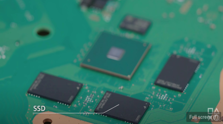
Maybe this? At the top:

vlcsnap-2020-10-07-16h53m33s380.png


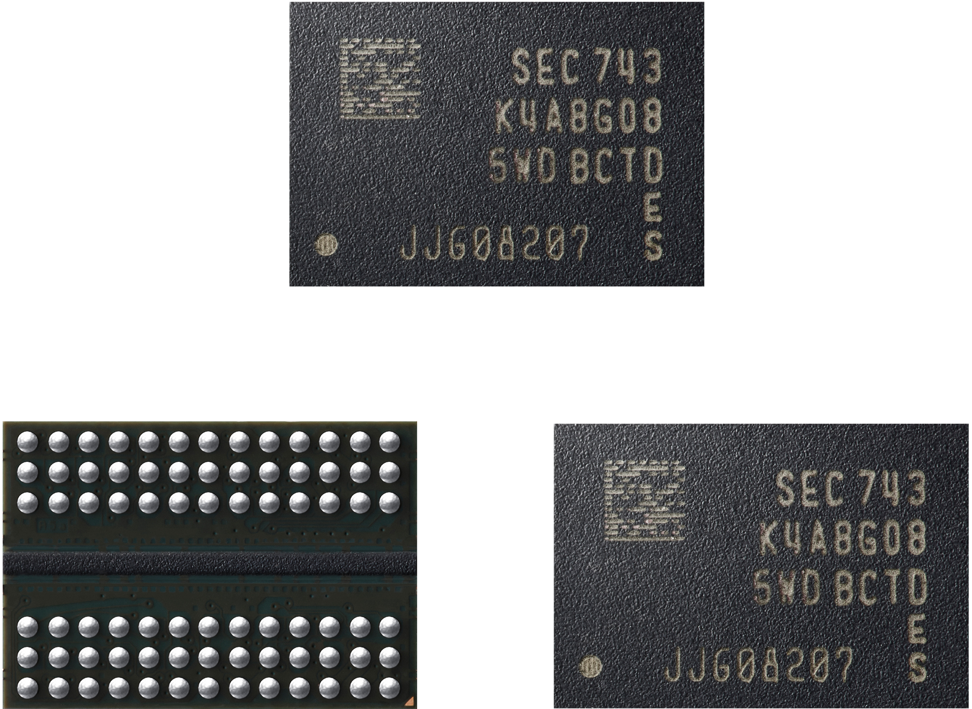
Samsung DDR4:

samsung_ddr4_10nm-v2-2.jpg


As it usually happens with Samsung’s major DRAM-related announcements, the news today consists of two parts: the first one is about the new DDR4 IC itself, the second part is about the second generation '10 nm-class' (which Samsung calls '1y' nm) manufacturing technology that will be used for other DRAM products by the company. Both parts are important, but let’s start with the new chip.


Or is it just DRAM and they are similarly looking?

Someone'd need to zoom in and sharpen the image a ton. Probably still wouldn't tell too much.

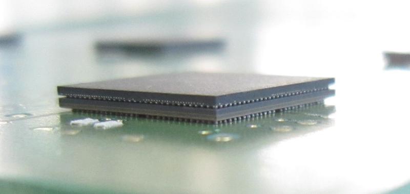
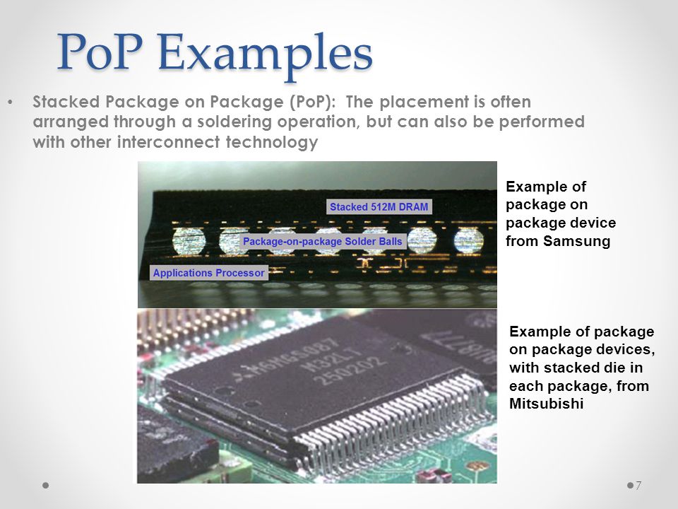
From what I know on POP (package-on-package) tech, it might be possible the DRAM cache is on top of the FMC, but you'd need some type of laminate substrate. So maybe the wider area is the substrate, but it looks a little too tightly packed between it and where the logic die would be?

Quickly, here's some shots of some POP and what (I guess) you'd usually look for:

9949828560_TIME_1448945837146.jpg


120612-escatec.jpg


PoP+Examples.jpg


Whatever's going on with the FMC in the PS5 shot there, doesn't look like POP.

As to the flash NAND, well the diagram at Road to PS5 did indeed show 12 chips as 12 channels, but the physical layout shot from PS5 teardown seems it only showed 6 chips. Maybe they are MCMs just physically joined to a single 256 GB package but each have their own channel connect direct to the FMC , instead of muxing two channels in the device to a single channel out to the FMC.

Because something like the latter, I think it would probably be drastic enough to require some statement or something we'd (eventually) hear about from a dev; it wouldn't really change performance metrics too much in the grand scheme of things, but it'd be notable enough in any case.
 
Last edited:

Tomeru

Member
Ok, people might get confused by the 22GB/s max. Whether they are raw or compressed, the SSD will send 5.5GB/s. Meaning, after decompression it results in 8-22GB/s inside the APU through the Kraken decompressor then to GPU caches and RAM:


So PCIe 4.0 could only handle 7GB/s, while PS5's SSD would send 5.5GB/s anyway through 4x PCIe 4.0 lanes. When it's inside the I/O complex, it gets decompressed to the original size, ranging from 8-22GB/s.

Hope this explains the concept.

I have no idea what you are talking about captain :messenger_tears_of_joy:
I think I should head to the infirmary!

Edit:
Ok, in a moment of seriousness, these kinds of discussions are great for reading, but I don't think anything weve seen so far explains any of them numbers. I am hype af though.
 
Last edited:

RaySoft

Member
Ok, people might get confused by the 22GB/s max. Whether they are raw or compressed, the SSD will send 5.5GB/s. Meaning, after decompression it results in 8-22GB/s inside the APU through the Kraken decompressor then to GPU caches and RAM:

ps5-custom-io-diagram-1584550561200.jpg


So PCIe 4.0 could only handle 7GB/s, while PS5's SSD would send 5.5GB/s anyway through 4x PCIe 4.0 lanes. When it's inside the I/O complex, it gets decompressed to the original size, ranging from 8-22GB/s.

Hope this explains the concept.
This i/o coupled with frustum culling equals MAGIC
 

Bo_Hazem

Banned
I have no idea what you are talking about captain :messenger_tears_of_joy:
I think I should head to the infirmary!

I guess this a simpler way of what's going on here: :lollipop_tears_of_joy:


Bo_Hazem

Banned
True it was absolutely a 2D system first and foremost, and arguably the last "true" 2D console (as in, having dedicated hardware specifically for 2D tiles and sprite manipulation). But, there's always been some dissenting over how much 3D was an afterthought for SEGA. Based on a few things I'm personally of the POV it wasn't really an afterthought, but the particular level of 3D they eventually got, was something of a last-minute thing.

Consider they not only had their Super-Scaler games in arcades from the mid-80s onwards (that used distorted sprites and was able to scale them quickly to simulate 3D...basically what the Saturn did with distorting quads), and also had their 3D arcade Virtua games by '93, I think that gives some credence to the idea at least Model 1-level 3D was always in the works for Saturn from the planning stages. They always tended to take aspects of their top-line arcade platforms of that era and placed into their home consoles, some things increased, some things stripped down, etc.

It's very hard to picture they would have designed Saturn in the early phases (when it was still called GigaDrive) without any 3D capabilities planned. However, their implementation was probably always going to be quad-based since that's what the arcade division was successful at with the Super-Scaler games (quad texture scaling) and Model 1 (using quadrilaterals for polygons, same thing Saturn would use). I'd probably even say some basic form of texture-mapping was also always in the works for Saturn, since it'd of came out in Japan after the Model 2 came out (IIRC the Model 2 actually put out less polygons than Model 1, but the texture mapping more than made up for it).

If Ken Kutaragi saw a game like Virtua Fighter and used that to convince Sony to commit to the PlayStation, I'm fairly sure the Away Team (the name of the team at SEGA assembled to develop the Saturn) were well enough aware of that game to take its 3D capabilities into the root of Saturn's design, balanced out with beefed-up 2D capabilities. The PS1 specs didn't so much force them to go with 3D, but attempt going with more robust 3D than what they were planning at the time.

Too bad the Away Team didn't have more time to tune the design; I honestly don't think dual processors (or dual VDPs) were necessarily the problem. SEGA's own teams were mastering those kind of setups for years. The problem was they never quite made the setup accessible enough for 3P devs in a gaming world that was quickly transforming, with publishers who needed games done faster (less reliance on assembly language coding). That's why I hope the concept of dual VDPs/dual-GPUs or whatever you want to call it, is perfected with multi-GPU chiplets becoming standard for a new generation of GPUs and consoles.

That's why I'm really interested in Intel's Xe architecture because IMO they're far ahead of AMD and Nvidia in that department. Too bad they've been a node behind them for a long time (and probably for foreseeable future), not even to mention what's been happening on the CPU front, AMD pretty much catching up to them if not surpassing them for the time being. It's gonna be a bit of a long road for Intel to regain their full footing but at least in the GPU space they've got a very strong foundation to work with.


Someone'd need to zoom in and sharpen the image a ton. Probably still wouldn't tell too much.

From what I know on POP (package-on-package) tech, it might be possible the DRAM cache is on top of the FMC, but you'd need some type of laminate substrate. So maybe the wider area is the substrate, but it looks a little too tightly packed between it and where the logic die would be?

Quickly, here's some shots of some POP and what (I guess) you'd usually look for:

9949828560_TIME_1448945837146.jpg


120612-escatec.jpg


PoP+Examples.jpg


Whatever's going on with the FMC in the PS5 shot there, doesn't look like POP.

As to the flash NAND, well the diagram at Road to PS5 did indeed show 12 chips as 12 channels, but the physical layout shot from PS5 teardown seems it only showed 6 chips. Maybe they are MCMs just physically joined to a single 256 GB package but each have their own channel connect direct to the FMC , instead of muxing two channels in the device to a single channel out to the FMC.

Because something like the latter, I think it would probably be drastic enough to require some statement or something we'd (eventually) hear about from a dev; it wouldn't really change performance metrics too much in the grand scheme of things, but it'd be notable enough in any case.

Ok, here is a shot, as some of them might be in the back of the motherboard. You have more experience in the matter and hope these would help you spot them all:

vlcsnap-2020-10-07-16h51m11s844.png


vlcsnap-2020-10-07-16h52m56s619.png


Could this mean that those are separated inside instead into 64x2MB?
 

RaySoft

Member
True it was absolutely a 2D system first and foremost, and arguably the last "true" 2D console (as in, having dedicated hardware specifically for 2D tiles and sprite manipulation). But, there's always been some dissenting over how much 3D was an afterthought for SEGA. Based on a few things I'm personally of the POV it wasn't really an afterthought, but the particular level of 3D they eventually got, was something of a last-minute thing.

Consider they not only had their Super-Scaler games in arcades from the mid-80s onwards (that used distorted sprites and was able to scale them quickly to simulate 3D...basically what the Saturn did with distorting quads), and also had their 3D arcade Virtua games by '93, I think that gives some credence to the idea at least Model 1-level 3D was always in the works for Saturn from the planning stages. They always tended to take aspects of their top-line arcade platforms of that era and placed into their home consoles, some things increased, some things stripped down, etc.

It's very hard to picture they would have designed Saturn in the early phases (when it was still called GigaDrive) without any 3D capabilities planned. However, their implementation was probably always going to be quad-based since that's what the arcade division was successful at with the Super-Scaler games (quad texture scaling) and Model 1 (using quadrilaterals for polygons, same thing Saturn would use). I'd probably even say some basic form of texture-mapping was also always in the works for Saturn, since it'd of came out in Japan after the Model 2 came out (IIRC the Model 2 actually put out less polygons than Model 1, but the texture mapping more than made up for it).

If Ken Kutaragi saw a game like Virtua Fighter and used that to convince Sony to commit to the PlayStation, I'm fairly sure the Away Team (the name of the team at SEGA assembled to develop the Saturn) were well enough aware of that game to take its 3D capabilities into the root of Saturn's design, balanced out with beefed-up 2D capabilities. The PS1 specs didn't so much force them to go with 3D, but attempt going with more robust 3D than what they were planning at the time.

Too bad the Away Team didn't have more time to tune the design; I honestly don't think dual processors (or dual VDPs) were necessarily the problem. SEGA's own teams were mastering those kind of setups for years. The problem was they never quite made the setup accessible enough for 3P devs in a gaming world that was quickly transforming, with publishers who needed games done faster (less reliance on assembly language coding). That's why I hope the concept of dual VDPs/dual-GPUs or whatever you want to call it, is perfected with multi-GPU chiplets becoming standard for a new generation of GPUs and consoles.

That's why I'm really interested in Intel's Xe architecture because IMO they're far ahead of AMD and Nvidia in that department. Too bad they've been a node behind them for a long time (and probably for foreseeable future), not even to mention what's been happening on the CPU front, AMD pretty much catching up to them if not surpassing them for the time being. It's gonna be a bit of a long road for Intel to regain their full footing but at least in the GPU space they've got a very strong foundation to work with.


Someone'd need to zoom in and sharpen the image a ton. Probably still wouldn't tell too much.

From what I know on POP (package-on-package) tech, it might be possible the DRAM cache is on top of the FMC, but you'd need some type of laminate substrate. So maybe the wider area is the substrate, but it looks a little too tightly packed between it and where the logic die would be?

Quickly, here's some shots of some POP and what (I guess) you'd usually look for:

9949828560_TIME_1448945837146.jpg


120612-escatec.jpg


PoP+Examples.jpg


Whatever's going on with the FMC in the PS5 shot there, doesn't look like POP.

As to the flash NAND, well the diagram at Road to PS5 did indeed show 12 chips as 12 channels, but the physical layout shot from PS5 teardown seems it only showed 6 chips. Maybe they are MCMs just physically joined to a single 256 GB package but each have their own channel connect direct to the FMC , instead of muxing two channels in the device to a single channel out to the FMC.

Because something like the latter, I think it would probably be drastic enough to require some statement or something we'd (eventually) hear about from a dev; it wouldn't really change performance metrics too much in the grand scheme of things, but it'd be notable enough in any case.
Really nice write-up!
You are 100% right, Sega fell into the same trap Sony did with the PS3, where they had extremely good knowledge of the hardware and a headstart of all other software companies. The sad part is that a console is dependant on 3rd party software, and when they must use a considerably time just for research, that's not a good sign. It doesn't help that "the other" console released at that time was cosiderably less hard to develop for. I usually love ecsotic hardware, but the times where not on Segas side that gen, unfortunately. We always cried "lazy devs" when they were handed some new piece of hardware that strayed a little from the beaten path, but in the end it's all about the money. I'm still certain though, without "some" ecsotic hardware there will be no progress, you just have to package it somewhat nicely for the devs to consume.
 
Last edited:

RaySoft

Member
Ok, people might get confused by the 22GB/s max. Whether they are raw or compressed, the SSD will send 5.5GB/s. Meaning, after decompression it results in 8-22GB/s inside the APU through the Kraken decompressor then to GPU caches and RAM:

ps5-custom-io-diagram-1584550561200.jpg


So PCIe 4.0 could only handle 7GB/s, while PS5's SSD would send 5.5GB/s anyway through 4x PCIe 4.0 lanes. When it's inside the I/O complex, it gets decompressed to the original size, ranging from 8-22GB/s.

Hope this explains the concept.
To simplify somewhat, the decompression hardware in the PS5 can output decompressed data at a peak rate of 22GB/s, meaning that even if the compression rate was even higher, the hardware itself couldn't "deliver" more than that ~22GB/s (probably a bit less since peak numbers are usually impossible to reach in real-world scenarios)
 

kyliethicc

Member
Maybe this? At the top:

vlcsnap-2020-10-07-16h53m33s380.png


Samsung DDR4:

samsung_ddr4_10nm-v2-2.jpg


As it usually happens with Samsung’s major DRAM-related announcements, the news today consists of two parts: the first one is about the new DDR4 IC itself, the second part is about the second generation '10 nm-class' (which Samsung calls '1y' nm) manufacturing technology that will be used for other DRAM products by the company. Both parts are important, but let’s start with the new chip.


Or is it just DRAM and they are similarly looking?

The PS5 flash controller clearly has a module of DDR4 SDRAM next to it. The 1 TB Samsung 980 Pro M.2 SSD has 1 GB (8 Gb) of Samsung LPDDR4 SDRAM on board for its controller. It looks like the PS5 has the same 1 GB chip, but it could be a different size. Hard to see. I've read that a DRAM cache can help improve read and write speeds. The Samsung 980 Pro 500 GB model only has 4 Gb or 512 MB DDR4, while I think I read the 2 TB model will have 2 GB (16 Gb) of cache. So I'd assume Sony is using 8 Gb.

The PS5 does have 6 flash dies for its SSD as thicc_girls_are_teh_best thicc_girls_are_teh_best said. It looks like its Toshiba 3D TLC NAND. Safe to assume all 6 dies are the same size, and since we know the PS5 is 768 GiB, then each flash chip is 128 GiB (1024 Gb.) And we know it uses 12 channels from the flash to the controller, and 4 lanes of PCIe 4.0 to the SOC.

The Samsung 980 Pro M2 SSD uses just 2 flash chips for its 1 TB model, which are Samsung 3D TLC NAND and 500 GB each, and it likely has 4 or 8 channels, same PCIe Gen4x4, with its own custom controller.
 

Bo_Hazem

Banned
The PS5 flash controller clearly has a module of DDR4 SDRAM next to it. The 1 TB Samsung 980 Pro M.2 SSD has 1 GB (8 Gb) of Samsung LPDDR4 SDRAM on board for its controller. It looks like the PS5 has the same 1 GB chip, but it could be a different size. Hard to see. I've read that a DRAM cache can help improve read and write speeds. The Samsung 980 Pro 500 GB model only has 4 Gb or 512 MB DDR4, while I think I read the 2 TB model will have 2 GB (16 Gb) of cache. So I'd assume Sony is using 8 Gb.

The PS5 does have 6 flash dies for its SSD as thicc_girls_are_teh_best thicc_girls_are_teh_best said. It looks like its Toshiba 3D TLC NAND. Safe to assume all 6 dies are the same size, and since we know the PS5 is 768 GiB, then each flash chip is 128 GiB (1024 Gb.) And we know it uses 12 channels from the flash to the controller, and 4 lanes of PCIe 4.0 to the SOC.

The Samsung 980 Pro M2 SSD uses just 2 flash chips for its 1 TB model, which are Samsung 3D TLC NAND and 500 GB each, and it likely has 4 or 8 channels, same PCIe Gen4x4, with its own custom controller.

I'm really confused, why did Cerny talk about 12 chips? Does this mean those are dual-chipped? Because he referred to 1 channel for each chip/module?
 

Tschumi

Member
So the only thing we can talk about is the efficiency. Than you should count in, that you don't want to compress texture data as one big chunk. Instead you want to compress only small chunks so you only need to load texture data into memory that is needed (PRT). Because of the small chunks and because of hardware based compression you loose efficiency on both sides.
I'm no expert, but isn't the elimination of this small chunk compression stuff one of the things Cerny said had been eliminated in the deep dive? Like it was one of the bottlenecks? Could be wrong~
 

Bo_Hazem

Banned
I'm no expert, but isn't the elimination of this small chunk compression stuff one of the things Cerny said had been eliminated in the deep dive? Like it was one of the bottlenecks? Could be wrong~

I think he was talking about compression of several assets in one compressed file. Well, that's not our job to decide how to do it, it's devs and studios.
 

Bo_Hazem

Banned
and here i recently just throwing money for "future proof" b550 pcie 4.0 motherboard

There is no such thing as future proofing in tech though. Future proofing extends to like 2-3 years max. You're lucky though my motherboard is PCIe 3.0. While it's sporting Radeon VII and Ryzen 2700x, it'll get trashed by PS5 by a great margin. My next PC would be built around PCIe 5.0 and should be capable enough to laugh at RAW 4K/8K 16-bit videos and uses 10-bit for snacks or I won't really upgrade. Currently it's pretty solid even crushing 4K videos up to 600fps or more.
 
Last edited:

Kumomeme

Member
There is no such thing as future proofing in tech though. Future proofing extends to like 2-3 years max. You're lucky though my motherboard is PCIe 3.0. While it's sporting Radeon VII and Ryzen 2700x, it'll get trashed by PS5 by a great margin. My next PC would be built around PCIe 5.0 and should be capable enough to laugh at RAW 4K/8K 16-bit videos and uses 10-bit for snacks or I won't really upgrade. Currently it's pretty solid even crushing 4K videos up to 600fps or more.
i know. it just i expect i could atleast last for 3 years before need to completely change new motherboard. other part like cpu and gpu should not have much issue as long the mobo still somehow supported.

but i doubt pcie 5.0 would come that soon. usually it gonna take place on place like servers first and it gonna be super expensive at first years.
 
Last edited:

Bo_Hazem

Banned
i know. it just i expect i could atleast last for 3 years before need to completely change new motherboard. other part like cpu and gpu should not have much issue.

but i doubt pcie 5.0 would come that soon. usually it gonna take place on place like servers and it gonna be super expensive at first years.

I think it'll come around 2022.
 

Stooky

Member
I think you will see gains with High quality assets vs resolution. If you look at film CG the vast majority of it is finished at 2k. Really any heavy effects movie or Cg animated film is finished in 2k. I think toy story 4 is the only animated film that was rendered in 4k. Jarrasic parks dinosaurs were rendered at 1k. The assets quality depends on how close that object is getting to the camera that can be from 2k up to 8k maps depending on detail thats needed, but yet only to finished at 2k lol. For me with the current state of computing I’ll take high quality assets over resolution.
 
Last edited:

Bo_Hazem

Banned
I think you will seen gains with High quality assets vs resolution. If you look at film CG the vast majority is finished at 2k. Really any heavy effects movie or Cg animated film is finished in 2k. In think toy story 4 is the only animated film that was rendered in 4k. Jarrasic parks dinosaurs were rendered at 1k. The assets quality depends on how close that object is getting to the camera that can be from 2k up to 8k maps depending on detail thats needed, but yet only to finished at 2k lol. For me with current state computing I’ll take high quality assets over resolution.

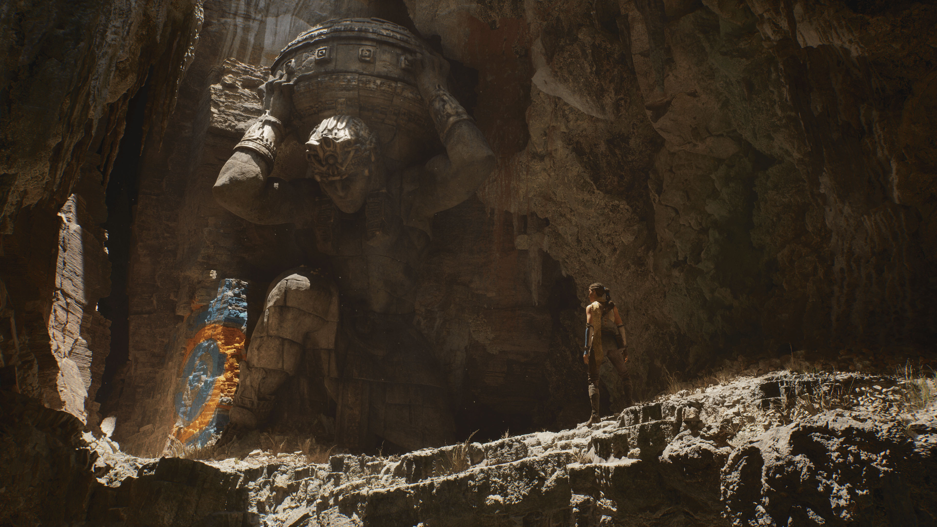
I will always take high quality assets over resolution, then probably AI reconstructed to 4K:

Unreal_Engine_5_13.jpg


But here, even 1080@60fps DMC5 on PS5 with RT still looks surprisingly solid and much better than Yakuza in 4K:

bluerose2_png_jpgcopy.jpg


redqueen2_png_jpgcopy.jpg


Bo_Hazem

Banned
I really cannot wait til this tech gets a public breakdown. Everyone is tripping saying that it's underpowered compared to the series X but are only paying attention to the most superficial specs and missing the forest for the trees

I believe it's already showing in the games we've seen from both sides so far.
 
He never actually said any of that, he just said 12 channels. It doesn't really matter, its a blazing fast SSD in the PS5.

That plus it just dawned on me; if volatile memory modules can have parallel multi-channels, then at this point I don't see why NAND modules can't.

The main disadvantage to larger-capacity, multi-channel NAND modules though is price; since they'd reduce the footprint of smaller NAND modules to be set on the PCB in parallel (I figure that could be resolved another way with PoP stacking, maybe), that real-estate savings will come at more of a premium.

Really nice write-up!
You are 100% right, Sega fell into the same trap Sony did with the PS3, where they had extremely good knowledge of the hardware and a headstart of all other software companies. The sad part is that a console is dependant on 3rd party software, and when they must use a considerably time just for research, that's not a good sign. It doesn't help that "the other" console released at that time was cosiderably less hard to develop for. I usually love ecsotic hardware, but the times where not on Segas side that gen, unfortunately. We always cried "lazy devs" when they were handed some new piece of hardware that strayed a little from the beaten path, but in the end it's all about the money. I'm still certain though, without "some" ecsotic hardware there will be no progress, you just have to package it somewhat nicely for the devs to consume.

Actually, there's something rather interesting on that. So by and large, PS1 definitely was easier to work on compared to Saturn, but that wasn't really so much about the architecture being considerably simpler. There's a small channel on YT I watch called Zygal Studios, they have some really good architectural breakdowns on retro systems for people interested.

The most recent one was for the PlayStation, and as you can tell it had it's own fair share of odd quirks and limitations. But it's like I was saying earlier: Sony had the resources and money to invest in a more mature SDK right out of the gate (plus less of those resources and money spread across other related product divisions), whereas SEGA needed almost a full year after Saturn's Japanese launch to do the same. They were probably similarly aware of the factor they were spending too much spread across to many product divisions in parallel, but they made the mistake of cutting the Genesis/MegaDrive short of what it could've been commercially; a 1996 Genesis/MegaDrive with full 1P support would've been amazing and eased the early transition into Saturn better. SoJ didn't care by then, though :( .

While SEGA were a bit more open/friendly with 3P devs than Nintendo at the time (some real horror stories regarding cartridge orders being massively late, order amounts drastically cut/reduced, not to mention limitations on how many games 3P devs could even develop/publish per-year, though they eased up on these things somewhat with SFC/SNES), the truth is both of them mainly used their hardware to push their own 1P titles; 3P who were able could hop along for the ride, but Nintendo and SEGA made few accommodations for them unless they were forced to (like when EA reverse-engineered the Genesis and forced SEGA to give them a premium licensing model else they'd release unofficial games for the system and, by doing so, probably encourage other 3P devs to try doing the same. Yeah, EA weren't the slimeball company back then they are today, but they still did some underhanded tactics).

Sony, out of necessity, were a lot more open to 3P devs and had the resources/money to drastically cheapen the manufacturing/distribution process for them, streamline the SDK so high-level languages could give results almost comparable with assembly (a lot of the better PS1 games still used assembly alongside C, though), and had a licensing model that was just cheaper than what Nintendo or even SEGA could've provided. Essentially, they used their corporate strengths and size to either force competitors to adapt (Nintendo), or burn cash trying (SEGA).

That's kind of what makes the current shift we're starting to see in the industry now so interesting, particularly for Sony, because if companies like Microsoft are now putting some actual money/resources towards game investment, as we can see in their Zenimax purchase, that's a long-term game Sony just can't compete in. Add in Apple, Google, Amazon etc.,...these are companies multiple sizes larger than a Sony or Nintendo. Nintendo's more or less secure since they've got a niche all their own and a fanbase who'll support it (as long as the hardware isn't completely botched like the Wii U).

It's going to be interesting to see how Sony adapts. Do they fully go into their own niche (and possibly lose some pure marketshare and 3P support but have other ways to retain or even grow profit margins) like Nintendo, or do they try braving against the Goliaths and play their game like SEGA tried doing with Sony in the mid '90s, because we saw what happened in the end there (sadly :( ). There are obvious differences between SEGA at that time and Sony right now, of course, but the overall main idea is the same: if it comes down to a battle of attrition, Sony loses simply because they have less money and resources to play the shopping game.

I personally think they'll manage; whether that comes through staying more or less completely of their own in gaming operations or establishing some type of partnership with one of these mammoth companies trying to capitalize on gaming's future is another question. Ironically this is why I say Microsoft stands more to lose if something were to happen to Sony, because the fact all three current platform holders look quite healthy, in it's own way is acting as a deterrent towards Apples, Amazon etc. from making a serious push into this particular gaming space (and that creates more trouble for Microsoft). I think MS understands this as well which is why, while I very much doubt you're ever going to see Zenimax/Bethesda games on Sony systems that aren't already promised or aren't MMO games (Death Loop, Elder Scrolls Online etc.) for example, it's that understanding why they're probably working with Sony in having PS5 leverage Azure going forward. It benefits Sony and ultimately also benefits MS, and it isn't something that impedes their plans in growing their own gaming product markets like Gamepass.

But for now I'm gonna finish watching this PS5 UI video they dropped out of nowhere overnight xD.
 
Last edited:

Bo_Hazem

Banned
That plus it just dawned on me; if volatile memory modules can have parallel multi-channels, then at this point I don't see why NAND modules can't.

The main disadvantage to larger-capacity, multi-channel NAND modules though is price; since they'd reduce the footprint of smaller NAND modules to be set on the PCB in parallel (I figure that could be resolved another way with PoP stacking, maybe), that real-estate savings will come at more of a premium.

I can really see some 12-channel per 12-module NVMe m.2 SSD's going forward if that's the case! Maybe that's why the bay has that very long compatible size? I would take something similar to the internal for 825GB over 7GB/s 2TB NVMe m.2 SSD with its deficiencies, except if I'm gonna use it as a away to offload games there quickly.
 
Last edited:
I can really see some 12-channel per 12-module NVMe m.2 SSD's going forward if that's the case! Maybe that's why the bay has that very long compatible size? I something similar to the internal for 825GB over 7GB/s 2TB NVMe m.2 SSD with its deficiencies, except if I'm gonna use it as a away to offload games there quickly.

Yeah that could happen and most likely will at some point. If I had to take bets, it'd probably be Samsung to make such a drive first, they seem to be at the forefront with high-end NVMe SSDs at the moment.

Technically speaking you'd be able to use such a drive as a means to play the games from it directly; it's only with drives connected through USB as external devices you can't use to play the games off of. Similar with the Series systems in that respect. That said, a 2 TB 7 GB/s (or faster) NVMe drive is going to cost $$$, especially if they go with the good NAND.
 

Bo_Hazem

Banned
Yeah that could happen and most likely will at some point. If I had to take bets, it'd probably be Samsung to make such a drive first, they seem to be at the forefront with high-end NVMe SSDs at the moment.

Technically speaking you'd be able to use such a drive as a means to play the games from it directly; it's only with drives connected through USB as external devices you can't use to play the games off of. Similar with the Series systems in that respect. That said, a 2 TB 7 GB/s (or faster) NVMe drive is going to cost $$$, especially if they go with the good NAND.

Yup, and prices gonna go down eventually, even for 2TB. As Cerny explains it, the I/O could use the extra speed of 7GB/s to compensate for the lack of 4 priority levels (2 vs 6 internally). But current top-tier NVMe m.2 SSD's tend to have 8-channel for 16 modules? If so it's a relation of 1:2 that might get data cramped and heat up the SSD.

I really want to know how that external one will be cooled.

You mean the external optional you can put internally? There looked to be a compartment for the optional internal SSD to allow for some cooling to pass through to it, so I'm assuming the system was already designed to provide cooling for such an option.

EDIT: Someone on B3D linked a 4gamer article with details on the PS5 teardown, but it's in Japanese only. They did pick out a few key things though, and maybe this:

-SSD slot can accept <8mm tall heatsink

Might be helpful?
 
Last edited:

Bo_Hazem

Banned
You mean the external optional you can put internally? There looked to be a compartment for the optional internal SSD to allow for some cooling to pass through to it, so I'm assuming the system was already designed to provide cooling for such an option.

EDIT: Someone on B3D linked a 4gamer article with details on the PS5 teardown, but it's in Japanese only. They did pick out a few key things though, and maybe this:


Might be helpful?

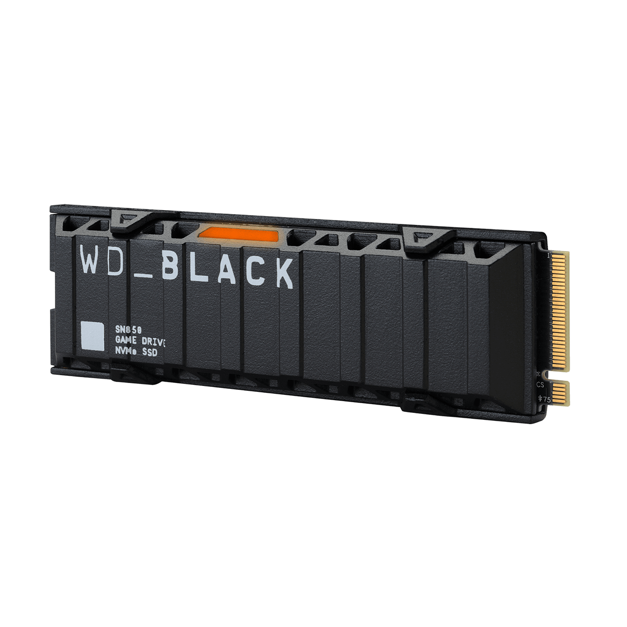
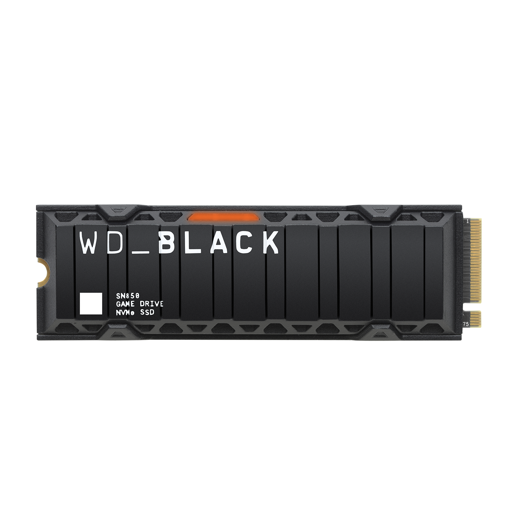
I think, let me check WD latest heatsink measurements:

wd-black-sn850-nvme-ssd-heatsink-side.png.thumb.1280.1280.png


I can see it being compatible? Or even take off the ceiling totally with a fan? I think there is enough room without that cover?

vlcsnap-2020-10-07-16h47m35s258.png


Not sure though, but good info! Thanks for sharing.
 
We now live in a world where having a more powerful GPU
That depends if the GPU's cache can effectively be filled up and updated efficiently for it to get as close to its theoretical peak performance. There are a few ways to improve it: (1) Make the cache really big, i.e. Infinity Cache, (2) design a system that only needs to invalidate a portion of the cache instead of evicting the entire cache, or (3) increase the cache bandwidth.

Faster CPU
That depends on how much CPU-intensive tasks are offloaded to dedicated, customized hardware. We know for a fact, for instance, that the PS5's decompression chip is more powerful than the XSX's decompression chip in terms of the number of Zen 2 cores offloaded.

Faster memory bandwidth are now "superficial specs". 🤣
That largely depends on the number of CU's that the RAM needs to feed data to. On a memory bandwidth per CU basis, the PS5 actually has an edge over the XSX. On a memory bandwidth per teraflop basis, the XSX has an edge over the PS5 albeit by a much smaller margin. The symmetry of the RAM layout will also affect how effective the RAM bandwidth is. The XSX will inevitably need to access the non-GPU optimized portion of the RAM pool, meaning that it will not be able to sustain the maximum 560 GB/s, especially if RAM usage exceeds 10GB. This will also cause the memory bandwidth per CU and per teraflop numbers to drop.
 

Bo_Hazem

Banned
That depends if the GPU's cache can effectively be filled up and updated efficiently for it to get as close to its theoretical peak performance. There are a few ways to improve it: (1) Make the cache really big, i.e. Infinity Cache, (2) design a system that only needs to invalidate a portion of the cache instead of evicting the entire cache, or (3) increase the cache bandwidth.


That depends on how much CPU-intensive tasks are offloaded to dedicated, customized hardware. We know for a fact, for instance, that the PS5's decompression chip is more powerful than the XSX's decompression chip in terms of the number of Zen 2 cores offloaded.


That largely depends on the number of CU's that the RAM needs to feed data to. On a memory bandwidth per CU basis, the PS5 actually has an edge over the XSX. On a memory bandwidth per teraflop basis, the XSX has an edge over the PS5 albeit by a much smaller margin. The symmetry of the RAM layout will also affect how effective the RAM bandwidth is. The XSX will inevitably need to access the non-GPU optimized portion of the RAM pool, meaning that it will not be able to sustain the maximum 560 GB/s, especially if RAM usage exceeds 10GB. This will also cause the memory bandwidth per CU and per teraflop numbers to drop.

Wonderful input. And the I/O throughput of 22GB/s makes the whole 825GB SSD like a DDR4 RAM! Which is insane:

DDR4 data rates: (single channel)

DDR4 2133: 17 GB / s
DDR4 2400: 19.2 GB / s
DDR4 2666: 21.3 GB / s

DDR4 3200: 25.6 GB / s


It's too fast that even without Oodle Texture the RAM needed a 0.7GB pool for streaming uncompressed 8K movie-level assets on the fly!
 
Last edited:
I'm seeing some confusion around the chips. The PS5 has 12 chips and one channel per chip correct?

EZx5Sf4XkAEBpOZ.jpg


I'm only seeing 6 chips on that board so they are probably stacked. So each chip is actually 2 of them.

PS5-899.jpg


There's three on the other side of the board.
 
Last edited:

Bo_Hazem

Banned
I'm seeing some confusion around the chips. The PS5 has 12 chips and one channel per chip correct?

EZx5Sf4XkAEBpOZ.jpg


I'm only seeing 6 chips on that board so they are probably stacked. So each chip is actually 2 of them.

PS5-899.jpg


There's three on the other side of the board.

I believe each has 2, that's the only answer. Mark Cerny isn't dumb to state that clearly with the graph and not be true. So those 6 must be packing 2x chips/modules each.
 
I believe each has 2, that's the only answer. Mark Cerny isn't dumb to state that clearly with the graph and not be true. So those 6 must be packing 2x chips/modules each.

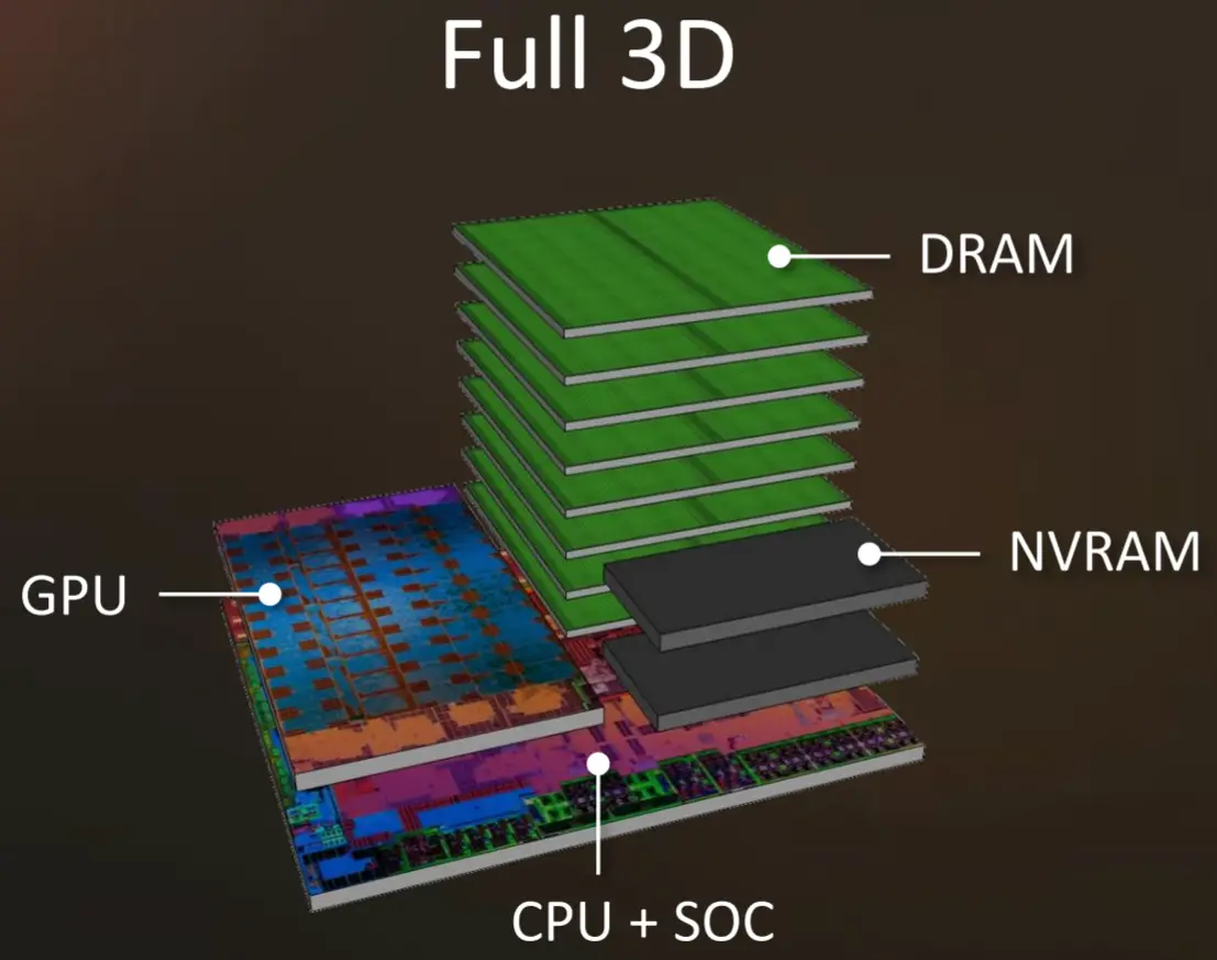
I don't know much about this but there's a technology called 3D stacking that can be applied to chips. I'm guessing something similar is happening here.

amd-iedm-2017-full-3d-stack.png
 

Bo_Hazem

Banned
Thanks to geordiemp geordiemp :

PS5 teardown in depth(Japanese)
https://www.4gamer.net/games/990/G999027/20201016035/

Some intesting point
-Sony used latest CAE technology to design the airflow inside PS5
-Chimney effect is at the measurement error level
-SSD slot can accept <8mm tall heatsink
-2 exhaust holes are provided for SSD slot, take the heat away by negative pressure
-not recommended to use heatsink that are high enough to touch the metal cover

Also ps5 DE is 0.95 x the volume of XSX (smaller but different shape.). Ps5 disk is 5 % bigger by volume.
 

clintar

Member
Thanks to geordiemp geordiemp :

PS5 teardown in depth(Japanese)
https://www.4gamer.net/games/990/G999027/20201016035/

Some intesting point
-Sony used latest CAE technology to design the airflow inside PS5
Correction:
CAE is sometimes used to optimize the airflow of each part, but it is not used in the overall design, and it is developed by conducting real experiments. Specifically, it is an image of making a transparent housing model and observing it by flowing dry ice smoke, or measuring the temperature of each part while making improvements.
 

Bo_Hazem

Banned
I don't know. I just thought it sounded a little different from what you were saying when I read it.

Well they used that to figure out the cooling of the system and monitor the air movement inside and through the components then out of the exhaust.
 

Bo_Hazem

Banned
The best news from that is that Unreal Engine 5 will have native support for RAD Tools.
So every multiplatform done with UE5 will automatically support these techs on PS5.

Above all of that Sony has already licensed Oodle Kraken and Oodle Texture for all PS5/PS4 devs so they can use them for free. Now with Epic Games having RAD Tools under their sleeves it'll make it the obvious choice across the board. It's pretty likely to throw BCPack and ZLIB out of the window for all 3rd party devs.
 
Top Bottom