• Hey, guest user. Hope you're enjoying NeoGAF! Have you considered registering for an account? Come join us and add your take to the daily discourse.

Xbox Velocity Architecture - 100 GB is instantly accessible by the developer through a custom hardware decompression block

Can you identify what each component of the APU is based on the image I posted above?;
Why? The ALU is the part n the centre, I’m not sure there are enough pixels there to resolve any “components” as such ( you would need a schematic or block diagram for that, not colors on a promotional image ). Unless you mean the RAM and a few diodes, resistors and capacitors around the ALU.
Do you know what an L1 cache is used for and why would it be any different on the above. Let’s just say you aren’t writing directly the results of memoized instruction to the L1 cache for a particular warp from an SSD as these are instruction level caches operating on either shared data for a particular fragment or array of fragments. The idea you are proposing isn’t based in reality because these are not caches as you know them, they cannot be known ahead of time to prewarm them.

That was a weird question in fairness, are you flexin'?
 
Last edited:

Tripolygon

Banned
Hold on a second, we discussed this before, what you just wrote is missing a few points.

Solution B wouldn't be using the same 64GB modules as Solution A. It can't add up to 825gb. 64x12 = 768! They are possibly using a variant of sram used in camera hardware ( which i could see sony doing considering they make cameras ) where one gb is represented as 1000 instead of 1024 ( i forget the name of mem type) , and that would give you a number closer to 825gb.
First of all no offence but you don't even have a basic grasp of this. No that's a variant of RAM used as cache. Its just simply conversion from binary to decimal system. They aren't using SRAM as Storage, SRAM is the cache used to store page data for wear leveling etc. They are using 512Gb or 64Gib X 12 = 768GiB convert it to Decimal system by multiplying by 1.074 = 825GB

You also aren't factoring in if either is using faster or slow memory modules ( that drives up the cost ) this is outside of the lane/channel bandwidth. They could be using anything from 800mt to 1600mt..
Secondly, no they won't be using anywhere near 1600MT/s NAND, that is DDR RAM territory of performance that does not exist in the storage space and also because the controller does not support it. Secondly bandwidth is derived from not just the speed of the controller itself but multiplied by the number of channels and NAND. I have done this math before on how i think they are achieving it. While being cost effective
Based on NAND catalog available out there looking through dramexchange, mouser and digikey from trying to piece together a possible BOM for both next gen consoles. My overhead of cost/performance is not wildly excessive its based on information out there from anywhere between 6% to 12% based on the level of correction you want in your storage system. Benchmark of DRAM-less SSDs are out there and show how drastic performance falls without a DRAM. My estimation is they are using 4 256GB at ~800MT/s NAND which gives them up to 3.2GB/s of bandwidth and ultimately arriving at 2.4GB/s as the sustained bandwidth taking all system overhead into consideration. Another option is using 667MT/s NAND which puts them at 2.6GB/s but I don't believe gives enough overhead.

Yes and that also factors into my speculation for how Sony are achieving their sustained bandwidth as well. 12 64GB NAND at 533MT/s which puts them at 6.3GB/s and accounting for the same overhead, well except for the SRAM in their IO complex, drops their bandwidth down to 5.5GB/s.

You also aren't factoring in the limitations on the technology and that is where "waste" comes in. It's not possible for any single mem module to use all available bandwidth if its on a single lane/channel. It introduces inefficiency that could play a factor in real-world vs on paper performance numbers.
What limitation? Not using the maximum capacity of a channel supported by the controller does not constitute as waste. The speed of the NAND you ultimately use determine your bandwidth multiplied by the number of channel.
 
Last edited:
Hold on a second, we discussed this before, what you just wrote is missing a few points.

Solution B wouldn't be using the same 64GB modules as Solution A. It can't add up to 825gb. 64x12 = 768! They are possibly using a variant of sram used in camera hardware ( which i could see sony doing considering they make cameras ) where one gb is represented as 1000 instead of 1024 ( i forget the name of mem type) , and that would give you a number closer to 825gb.

You also aren't factoring in if either is using faster or slow memory modules ( that drives up the cost ) this is outside of the lane/channel bandwidth. They could be using anything from 800mt to 1600mt. You also aren't factoring in the limitations on the technology and that is where "waste" comes in. It's not possible for any single mem module to use all available bandwidth if its on a single lane/channel. It introduces inefficiency that could play a factor in real-world vs on paper performance numbers.

The 825 GB figure is actually really weird. There's Gigabyte and Gibibyte. A Gibibyte is 1024 Mebibytes, and 1073741824bytes = 1024 mebibytes.

Sony's basically converting Gigabytes to Gibibytes to reach the 825 GB claim, but using GB instead of GiB. 768 GB x 1.073 (the rounded value of 1 Gibibyte to 1 Gigabyte) = 824.064 "GB", about the 825 number Sony provides. 768 GB / 12 = 64 GB, so Sony are using 12 64 GB flash modules providing 768 gigabytes, but 825 "gibibytes".

Tripolygon Tripolygon For your assumed NAND chip calculations, the part you're wrong is figuring the 2.4 GB/s comes from reduction due to system overhead. There is no amount of system overhead that requires a 800 MB/s lost, period!

The flash memory controller in XSX is likely rated at 5 GB/s, so it has to service both the internal and expansion storage, presumed simultaneously if both are present in the system. 2.4 GB/s to both = 4.8 GB/s total. PCIe 4.0 uses 128b/130b encoding so very little (less than 5 MB) is actually lost to raw overhead per lane, and I'd be remiss if the XSX OS is so bloated it needs to gargle away another 795 MB of SSD bandwidth on the controller simply to manage them.

It's the other way around. They have 768 gibibytes, but 826gigabytes.
Otherwise it's correct

Actually this is kinda funny because some companies seem to actually do the inverse! The IEC changed the standardization of definition a few years ago IIRC, but maybe many others still roll with the older way?

Places I've looked at seem to go with Gibibyte as 1.073 (or 1.074)x Gigabyte, and swap their bases. But due to that a company may specify gibibyte but still use GB as shorthand instead of GiB which would be the actual correct usage in that case.

It's a bit confusing :S
 
Last edited:

THE:MILKMAN

Member
Can you identify what each component of the APU is based on the image I posted above?;

Can I try/guess?

Blue = 2x Zen 2 CCX, logic between is IF/decompression chip/IO etc
Green = 56(52)CUs
Memory controllers along left/right/top
 
Last edited:

Ascend

Member
Why? The ALU is the part n the centre, I’m not sure there are enough pixels there to resolve any “components” as such. Unless you mean the RAM and a few diodes, resistors and capacitors around the ALU.
Do you know what an L1 cache is used for and why would it be any different on the above. Let’s just say you aren’t writing directly the results of memoized instruction to the L1 cache for a particular warp on an SSD as these are instruction level caches operating on either shared data for a particular fragment or array of fragments. The idea you are proposing isn’t based in reality because these are not caches as you know them, they cannot be known ahead of time to prewarm them.
I meant more like, what are the blue parts and what is the green part, and what do they consist of?

The easiest one is the blue ones, which look like the two core complexes of the CPU.
The green one looks like the GPU, but it's harder to discern what's on it. The large box looks like the CUs, while the two 'outer' green boxes on the top of the large box are likely the L1 cache + mesh shaders. The one in the middle would be the command processor.
Then we have those rectangular things on the sides, which are likely the memory controllers, L2 cache, PCIe connectors etc.

Obviously I'm not expecting transfer from SSD to L1 cache. But if you're going to use 64kb sized mip regions, and you have to transfer those from the SSD, why would you send that to RAM first, rather than the L2 cache (or whatever the largest cache will be)? To me they seem small enough, and sending it to RAM would add unnecessary latency. I could be wrong though.

That was a weird question in fairness, are you flexin'?
I thought maybe you could identify more of it than me, since you seem more knowledgeable.
 
Last edited:
The 825 GB figure is actually really weird. There's Gigabyte and Gibibyte. A Gibibyte is 1024 Mebibytes, and 1073741824bytes = 1024 mebibytes.

Sony's basically converting Gigabytes to Gibibytes to reach the 825 GB claim, but using GB instead of GiB. 768 GB x 1.073 (the rounded value of 1 Gibibyte to 1 Gigabyte) = 824.064 "GB", about the 825 number Sony provides. 768 GB / 12 = 64 GB, so Sony are using 12 64 GB flash modules providing 768 gigabytes, but 825 "gibibytes".

Tripolygon Tripolygon For your assumed NAND chip calculations, the part you're wrong is figuring the 2.4 GB/s comes from reduction due to system overhead. There is no amount of system overhead that requires a 800 MB/s lost, period!

The flash memory controller in XSX is likely rated at 5 GB/s, so it has to service both the internal and expansion storage, presumed simultaneously if both are present in the system. 2.4 GB/s to both = 4.8 GB/s total. PCIe 4.0 uses 128b/130b encoding so very little (less than 5 MB) is actually lost to raw overhead per lane, and I'd be remiss if the XSX OS is so bloated it needs to gargle away another 795 MB of SSD bandwidth on the controller simply to manage them.
It's the other way around. They have 768 gibibytes, but 825 gigabytes.
Otherwise it's correct
 
Last edited:
I meant more like, what are the blue parts and what is the green part, and what do they consist of?

The easiest one is the blue ones, which look like the two core complexes of the CPU.
The green one looks like the GPU, but it's harder to discern what's on it. The large box looks like the CUs, while the two 'outer' green boxes on the top of the large box are likely the L1 cache + mesh shaders. The one in the middle would be the command processor.
Then we have those rectangular things on the sides, which are likely the memory controllers, L2 cache, PCIe connectors etc.

Obviously I'm not expecting transfer from SSD to L1 cache. But if you're going to use 64kb sized mip regions, and you have to transfer those from the SSD, why would you send that to RAM first, rather than the L2 cache? To me they seem small enough, and sending it to RAM would add unnecessary latency. I could be wrong though.

I wouldn't use colored in marketing images to guess anything like that, wait for a real block diagram to come out.

It's the instructions running that decide if they are using that MIP level, so they would load into RAM, then cache, and multiple threads work on it. The cache isn't waiting idle for an SSD to load data. Remember, you have 1000's of threads writing different parts of cache depending on how and when they are scheduled, billions of times a second! You aren't going to ask an SSD to help here and bulldoze over all instruction cache? Then you swizzle it to a shared pointer used by a running set of instructions? It's weird. The RAM is what you want in this case. A shader developer specifics global, shared or local data themselves, which corresponds to where it may be placed.
 

Tripolygon

Banned
Tripolygon Tripolygon For your assumed NAND chip calculations, the part you're wrong is figuring the 2.4 GB/s comes from reduction due to system overhead. There is no amount of system overhead that requires a 800 MB/s lost, period!
And I disagree, using a nand that gives them 2.4GB/s or 2.6GB/s does not give enough overhead that accounts for the fact that their controller is DRAM-less, nor does it account for bandwidth degradation based on thermal throttling, ECC etc. Period!
 

Ascend

Member
I wouldn't use colored in marketing images to guess anything like that, wait for a real block diagram to come out.

It's the instructions running that decide if they are using that MIP level, so they would load into RAM, then cache, and multiple threads work on it. The cache isn't waiting idle for an SSD to load data. Remember, you have 1000's of threads writing different parts of cache depending on how and when they are scheduled, billions of times a second! You aren't going to ask an SSD to help here and bulldoze over all instruction cache? Then you swizzle it to a shared pointer used by a running set of instructions? It's weird. The RAM is what you want in this case. A shader developer specifics global, shared or local data themselves, which corresponds to where it may be placed.
Ok. Just a few questions...

If you have a cache miss, isn't that equivalent to the cache waiting idle for the data to load?
Why would loading from the SSD bulldoze over all instruction cache more than RAM would?
 
And I disagree, using a nand that gives them 2.4GB/s or 2.6GB/s does not give enough overhead that accounts for the fact that their controller is DRAM-less, nor does it account for bandwidth degradation based on thermal throttling, ECC etc. Period!

They gave the 2.4 GB/s as a sustained number that already accounts for throttling. That's the guaranteed performance of raw data performance on the drive under heavy loads; it can peak higher but those (especially some of those) are edge cases. If operations don't need to transfer 2.4 GB in a second, that isn't a case of throttling, just the fact lesser data than the rated sustained peak is require for that operation.

Having DRAM-less SSD does not result in a 800 MB/s drop, that's kind of ridiculous to assume. A portion of the system's GDDR6 (some of the 2.5 GB reserved for the OS) is being used as cache of data to/from the SSD I'm assuming, and FWIW the PS5 does not have DRAM in its memory controller (flash), either. They are using SRAM, which won't top out beyond a small portion (4 - 8 MB tops) since if it's true SRAM it's going to be expensive. So where is the assumed overhead taken into account for that instance?

How do you presume to know the way ECC works? There are actually NAND modules with built-in ECC to their design; this doesn't seem to be an area in regards engineering MS would screw up and overlook, only to find out afterwards it's contributing to some 800 MB/s bandwidth loss (never mind then thinking they're okay with sticking with such).

There's no "period!" here; you're just completely off-base on this particular aspect of the system.
 
Actually this is kinda funny because some companies seem to actually do the inverse! The IEC changed the standardization of definition a few years ago IIRC, but maybe many others still roll with the older way?

Places I've looked at seem to go with Gibibyte as 1.073 (or 1.074)x Gigabyte, and swap their bases. But due to that a company may specify gibibyte but still use GB as shorthand instead of GiB which would be the actual correct usage in that case.

It's a bit confusing :S
Yeah that's true.
 
Ok. Just a few questions...

If you have a cache miss, isn't that equivalent to the cache waiting idle for the data to load?
Why would loading from the SSD bulldoze over all instruction cache more than RAM would?
It falls back to L2 cache then RAM, and yes that would cause stalls if it happened all the time. The data missed from cache is usually a few bytes, so loading 64kb of data into a cache that you don’t know is being used is overkill. Remember these are data structures and memoized functions being stored in these caches which have been defined by the runtime code. When you write you do not write to cache but to RAM. Only on read is it then cached (Readthrough caching)
look up load/store in shader code in relation to caches for more info, don’t take my word for it.
 
Last edited:

Ascend

Member
It falls back to L2 cache then RAM, and yes that would cause stalls if it happened all the time. The data missed from cache is usually a few bytes, so loading 64kb of data into a cache that you don’t know is being used is overkill. Remember these are data structures and memoized functions being stored in these caches which have been defined by the runtime code. When you write you do not write to cache but to RAM. Only on read is it then cached (Readthrough caching)
look up load/store in shader code in relation to caches for more info, don’t take my word for it.
So we're on the same page (no pun intended). I guess some of the confusion was on the semantics.

The thing is though, going back to what we were discussing earlier, if 100GB of SSD data is seen as RAM by the system, and we assume everything is still only on the SSD, you would not have to actually read L1 -> L2 -> RAM -> Storage, you would only need to read L1 -> L2 -> "RAM" (which is actually the 100GB on the SSD). If you actually implement the virtual RAM in software for the 100GB, you will create additional overhead afaik, and I don't think that would quality as 'instantly accessible'.
So maybe rather than me wording it writing to cache, maybe I should have said bypassing the 16GB of RAM on read.
 
Last edited:

Tripolygon

Banned
They gave the 2.4 GB/s as a sustained number that already accounts for throttling. That's the guaranteed performance of raw data performance on the drive under heavy loads; it can peak higher but those (especially some of those) are edge cases. If operations don't need to transfer 2.4 GB in a second, that isn't a case of throttling, just the fact lesser data than the rated sustained peak is require for that operation.
Yes they gave 2.4GB/s as their sustained speed that accounts for every overhead and I'm postulating that to achieve their 2.4GB/s sustained performance, they are using nand modules faster than that which accounts for those overhead.


Having DRAM-less SSD does not result in a 800 MB/s drop, that's kind of ridiculous to assume. A portion of the system's GDDR6 (some of the 2.5 GB reserved for the OS) is being used as cache of data to/from the SSD I'm assuming,
Or they aren't trying to reduce their RAM bandwidth further by adding another source of contention instead of using part of their SSD that is slightly faster as page cache.

and FWIW the PS5 does not have DRAM in its memory controller (flash), either. They are using SRAM, which won't top out beyond a small portion (4 - 8 MB tops) since if it's true SRAM it's going to be expensive. So where is the assumed overhead taken into account for that instance?
4 to 6MB tops where? Mr Cerny said they provide a generous amount of SRAM, there whole patent talks about using SRAM instead of DRAM and it takes up quite a bit of the IO complex.

How do you presume to know the way ECC works? There are actually NAND modules with built-in ECC to their design; this doesn't seem to be an area in regards engineering MS would screw up and overlook, only to find out afterwards it's contributing to some 800 MB/s bandwidth loss (never mind then thinking they're okay with sticking with such).
Ever heard of the novel concept of reading? I don't presume to know everything, i know some stuff and from my limited knowledge I make semi educated guess. You can disagree and that is fine and i disagree with your disagree. The breakdown of the system will tell the whole story and i could be wrong and that's fine too it would not be the first time i was wrong about something for example i thought next gen consoles will have Zen 1 CPU clocked at most 2.8GHz, i was wrong, i thought next gen consoles will have 52CU clocked at 1.6Ghz to give around 10TF and again I was wrong. The world keeps turning.

There's no "period!" here; you're just completely off-base on this particular aspect of the system.
Period! I have made my speculations which are within the bounds of reason and its not really up for debate. I could entirely be wrong and I'm not trying to convince you otherwise. I made my speculations based on what I know.
 
So we're on the same page (no pun intended). I guess some of the confusion was on the semantics.

The thing is though, going back to what we were discussing earlier, if 100GB of SSD data is seen as RAM by the system, and we assume everything is still only on the SSD, you would not have to actually read L1 -> L2 -> RAM -> Storage, you would only need to read L1 -> L2 -> "RAM" (which is actually the 100GB on the SSD). If you actually implement the virtual RAM in software for the 100GB, you will create additional overhead afaik, and I don't think that would quality as 'instantly accessible'.
So maybe rather than me wording it writing to cache, maybe I should have said bypassing the 16GB of RAM on read.
That would kill performance if done that late, you need everything in RAM before you execute the next set of instructions. But you are getting closer, it’s at the next frame we then load from the SSD when we require new data for the frame. Latency and speed here is crucial and have a 100gb swap ready means we can memory map it and treat it as RAM for quicker access. You need a fast drive for this to perform well in under 33ms.
Finally though, this is not a new tech exclusive to Xbox, there is nothing stopping Sony doing the same for PlayStation. I mean, every OS in the world does it already, just not to this level as you can’t guarantee the hardware like you can a console.
 

oldergamer

Member
First of all no offence but you don't even have a basic grasp of this. No that's a variant of RAM used as cache. Its just simply conversion from binary to decimal system. They aren't using SRAM as Storage, SRAM is the cache used to store page data for wear leveling etc. They are using 512Gb or 64Gib X 12 = 768GiB convert it to Decimal system by multiplying by 1.074 = 825GB
Hey I'm not claiming to have all the answers and know only what i've read on this recently. You're right, and what you wrote is in line with what i read before and totally forgot. I was groggy after waking up when i wrote SRAM, i should have said NAND specifically.

Secondly, no they won't be using anywhere near 1600MT/s NAND, that is DDR RAM territory of performance that does not exist in the storage space and also because the controller does not support it. Secondly bandwidth is derived from not just the speed of the controller itself but multiplied by the number of channels and NAND. I have done this math before on how i think they are achieving it. While being cost effective
1200MT has been the maximum due to signal integrity issues, however some companies have developed controllers that allow for up to 1600MT and no I wasn't specifically talking about DDR RAM
Am i still wrong?

What limitation? Not using the maximum capacity of a channel supported by the controller does not constitute as waste. The speed of the NAND you ultimately use determine your bandwidth multiplied by the number of channel.
Did i originally claim it as "waste" or did I say it was inefficient? note i was quoting someone else calling it "waste".

if you say so, the article i read specifically called out using a single channel per NAND module as inefficient.
 
Last edited:

Ascend

Member
That would kill performance if done that late, you need everything in RAM before you execute the next set of instructions. But you are getting closer, it’s at the next frame we then load from the SSD when we require new data for the frame.
I am aware of that. I was just creating an isolated scenario to be as clear as possible on what I mean.

Latency and speed here is crucial and have a 100gb swap ready means we can memory map it and treat it as RAM for quicker access. You need a fast drive for this to perform well in under 33ms.
2.4GB/s would mean 40MB of raw data per frame at 60fps. If you have 64kb mips, that would mean about 10 mips per frame. Add in the compression and you can get almost 20. If the PS5 can do the same, it would be about 35 mips per frame. Just brainstorming here. Don't mind me lol.

Finally though, this is not a new tech exclusive to Xbox, there is nothing stopping Sony doing the same for PlayStation. I mean, every OS in the world does it already, just not to this level as you can’t guarantee the hardware like you can a console.
Could this be accelerated with hardware to reduce overhead, rather than doing it in software? I assume it's what the DirectStorage API is for, rather than any hardware, but, just asking.
 
I am aware of that. I was just creating an isolated scenario to be as clear as possible on what I mean.


2.4GB/s would mean 40MB of raw data per frame at 60fps. If you have 64kb mips, that would mean about 10 mips per frame. Add in the compression and you can get almost 20. If the PS5 can do the same, it would be about 35 mips per frame. Just brainstorming here. Don't mind me lol.


Could this be accelerated with hardware to reduce overhead, rather than doing it in software? I assume it's what the DirectStorage API is for, rather than any hardware, but, just asking.
Yes it is, and PS5 has the advantage here as low latency means you don’t need full speed, you just need the data earlier and you may not need much of it. Coupling the fact that you can have data in RAM earlier with the fact you need less data in the first place is what makes this an interesting prospect. Engines such as UE5 which optimise the data fetched and yes things like SFS will mean you don’t need to rely on bandwidth so much, but getting the data you need as quick as possible. We want smaller payloads ASAP. Bandwidth helps with other aspects though.
 

oldergamer

Member
Totally missed this:

"Sony's basically converting Gigabytes to Gibibytes to reach the 825 GB claim, but using GB instead of GiB. 768 GB x 1.073 (the rounded value of 1 Gibibyte to 1 Gigabyte) = 824.064 "GB", about the 825 number Sony provides. 768 GB / 12 = 64 GB, so Sony are using 12 64 GB flash modules providing 768 gigabytes, but 825 "gibibytes"."

yeah i got confused with this. Actually is this correct?

768 gigabytes = 715.256 gibibytes when i do a conversion in google

Scratch that. I didn't hit enter. 768 gibibytes = 825 gigabytes.
 

Fafalada

Fafracer forever
Obviously I'm not expecting transfer from SSD to L1 cache. But if you're going to use 64kb sized mip regions, and you have to transfer those from the SSD, why would you send that to RAM first, rather than the L2 cache (or whatever the largest cache will be)? To me they seem small enough, and sending it to RAM would add unnecessary latency.
What you're proposing is Scratch-pad like workflow (or Cell SPEs for a more recent example) the problem is the latency gulf between SSD and memory is several orders of magnitude larger than memory:cache ratio where these are normally applied, and synchronization/handling direct requests from a massively parallel consumer like GPU is a problem I'm not even sure has a viable solution.

Eg: reading direct to L2 would require exact knowledge of requested addresses for every 64KB block (or smaller) just in time for the GPU to use it - meaning you're doing this several thousand times per frame, putting the latency required for each read into micro-seconds range.
Now consider that the flaunted SFS that's supposed to do something like this in hardware - proposes to work on previous frame to prepare 'what's needed' - meaning it operates on a latency in 10s of mili-seconds - which makes it at least 1000x too slow for the above.
That's before looking at whether the SSD can theoretically keep up with this either (64K granularity would mean 120000 IOP/s just for cache refills, double that for 32KB and so on).
Finally - assuming we locked the entire cache - this would turn the GPU workflow into how Cell used to do things (Every piece of data had to be pre-fetched manually, by the developer). Alternatively - if you lock only a portion (50%?) of the cache you've just reduced the efficiency of everything else GPU does (that doesn't rely on your pre-fetching area) by whatever the size-portion of cache you lost to this.

And all that's still grossly oversimplifying the scope of the problem (address reads aren't in 10+ KB granularity, and I assumed 100% cache-hitrate in numbers above, it'd only get worse in real-world) . The synchronization complexity nightmare I mentioned in first paragraph I just skimmed over for the sake of argument. Even looking at CPUs where similar mechanisms existed since the 90s, cache-line locking was in simple scenarios where you only have one serial-consumer. Don't think we ever got this for shared-cache setups in multi-core designs as the synchronization complexity there already overshadows whatever latency benefits you might get from explicitly feeding the cache. And GPU makes that orders of magnitude worse.
 
Last edited:

Tripolygon

Banned
Hey I'm not claiming to have all the answers and know only what i've read on this recently. You're right, and what you wrote is in line with what i read before and totally forgot. I was groggy after waking up when i wrote SRAM, i should have said NAND specifically.
That's cool. I misunderstand and misquote things all the time too.

1200MT has been the maximum due to signal integrity issues, however some companies have developed controllers that allow for up to 1600MT and no I wasn't specifically talking about DDR RAM
Am i still wrong?
Storage, specifically consumer space sector has not seen any need for nand at those speeds. We are just barely now reaching 5GB/s storage speed. Enterprise and server side are what use those types of speeds.

Did i originally claim it as "waste" or did I say it was inefficient? note i was quoting someone else calling it "waste".
It is neither waste nor inefficient. There design is straightforward, they want to achieve high bandwidth and the simplest way to do that without having to deal with interleaving which adds another complexity is to dedicate 1 channel per NAND. Its not a waste nor inefficient, just straightforward.

if you say so, the article i read specifically called out using a single channel per NAND module as inefficient.
Inefficient is relative here to what you are trying to achieve. I don't think Console manufactures like inefficiency, they count everything based on the cost to produce vs output.
 
Last edited:

Ascend

Member
What you're proposing is Scratch-pad like workflow (or Cell SPEs for a more recent example) the problem is the latency gulf between SSD and memory is several orders of magnitude larger than memory:cache ratio where these are normally applied, and synchronization/handling direct requests from a massively parallel consumer like GPU is a problem I'm not even sure has a viable solution.
You might be right.

reading direct to L2 would require exact knowledge of requested addresses for every 64KB block (or smaller) just in time for the GPU to use it
That is exactly what MS is advertising with SFS, except they said into memory, not cache...;

Sampler Feedback Streaming (SFS) – A component of the Xbox Velocity Architecture, SFS is a feature of the Xbox Series X hardware that allows games to load into memory, with fine granularity, only the portions of textures that the GPU needs for a scene, as it needs it.

They didn't say it was RAM, although mostly when one says memory, it's implied that it's RAM. The thing is that they consider 100GB of the SSD as 'extended' memory, i.e. the system does not differentiate between the 16GB of RAM and the 100GB of the SSD, which is what started this speculation that the XSX could read directly from SSD without needing the RAM. Obviously not only from the SSD and not all the time...

- meaning you're doing this several thousand times per frame, putting the latency required for each read into micro-seconds range.
Now consider that the flaunted SFS that's supposed to do something like this in hardware - proposes to work on previous frame to prepare 'what's needed' - meaning it operates on a latency in 10s of mili-seconds - which makes it at least 1000x too slow for the above.
That is why they say a lower quality mip is guaranteed to be in place (likely cached in advance from memory), given the high quality mip a chance to finish loading;

A technique called Sampler Feedback Streaming - SFS - was built to more closely marry the memory demands of the GPU, intelligently loading in the texture mip data that's actually required with the guarantee of a lower quality mip available if the higher quality version isn't readily available, stopping GPU stalls and frame-time spikes. Bespoke hardware within the GPU is available to smooth the transition between mips, on the off-chance that the higher quality texture arrives a frame or two later.

That's before looking at whether the SSD can theoretically keep up with this either (64K granularity would mean 120000 IOP/s just for cache refills, double that for 32KB and so on).
That doesn't seem outside of the realm of possibility... As an example, a 960 EVO can do 380k IOPS. That seems quite average for NVMe SSD drives. Good SATA drives are in the range of 100k IOPS.

Finally - assuming we locked the entire cache - this would turn the GPU workflow into how Cell used to do things (Every piece of data had to be pre-fetched manually, by the developer). Alternatively - if you lock only a portion (50%?) of the cache you've just reduced the efficiency of everything else GPU does (that doesn't rely on your pre-fetching area) by whatever the size-portion of cache you lost to this.
This is true. But what else would take so much space for the GPU cache? Aren't the mips the largest chunks of data?

And all that's still grossly oversimplifying the scope of the problem (address reads aren't in 10+ KB granularity, and I assumed 100% cache-hitrate in numbers above, it'd only get worse in real-world) . The synchronization complexity nightmare I mentioned in first paragraph I just skimmed over for the sake of argument. Even looking at CPUs where similar mechanisms existed since the 90s, cache-line locking was in simple scenarios where you only have one serial-consumer. Don't think we ever got this for shared-cache setups in multi-core designs as the synchronization complexity there already overshadows whatever latency benefits you might get from explicitly feeding the cache. And GPU makes that orders of magnitude worse.
Just like you could theoretically lock a portion of the GPU cache as you mentioned above, you can lock a portion of the shared cache for the CPU, and leave the rest for the GPU (or vice versa). The main drawback I see is that you can have duplicate data, effectively reducing cache size. That could possibly happen in the other scenario we discussed above as well.
 
Yes they gave 2.4GB/s as their sustained speed that accounts for every overhead and I'm postulating that to achieve their 2.4GB/s sustained performance, they are using nand modules faster than that which accounts for those overhead.

If they are using NAND modules faster than what the controller can handle, they aren't THAT much faster. Again, the controller is designed to provide sustained 2.4 GB/s to BOTH the internal drive and an external expansion card inserted.

I highly doubt MS would spend money on NAND modules giving them an excess 800 MB/s bandwidth that just goes to waste. No company, not even a laughing stock like modern-day Atari, would be stupid enough to waste that type of money. Insinuating a company as experienced and entrenched as Microsoft would do so is laughable.

Or they aren't trying to reduce their RAM bandwidth further by adding another source of contention instead of using part of their SSD that is slightly faster as page cache.

This is possible; I've speculated they could have a cache of SLC NAND on the drive, but have speculated this could be related to the 100 GB partition they've mentioned previously for "instant" (don't think speed here, think reduction of steps in getting from Point A to Point B) access by the GPU.

It's possible that it could be doing this, or both. Or, again, they could be using a bit of the reserved 2.5 GB to the OS for it, or all of these things in tandem. We don't know yet.

4 to 6MB tops where? Mr Cerny said they provide a generous amount of SRAM, there whole patent talks about using SRAM instead of DRAM and it takes up quite a bit of the IO complex.

"Generous amount" can mean anything. Additionally, SRAM tends to take up a lot of die space. Let's assume the XBO's ESRAM; it took up a big chunk of the APU and that was 32 MB's worth. Realistically you're looking at 4-8 MB of SRAM if it's true SRAM and the high-quality sort being embedded into the I/O block. If it's lower-quality SRAM, they cam possibly double that size.

If they're using pseudo-SRAM (PSRAM), they can probably get 32 MB or even 64 MB. But that's it. And even 64 MB of PSRAM, comparatively speaking, is much smaller than the typical DRAM cache sizes on higher-end NVMe SSD drives. That's part of the tradeoff in going with SRAM over DRAM: smaller capacity, but faster speed.

Ever heard of the novel concept of reading? I don't presume to know everything, i know some stuff and from my limited knowledge I make semi educated guess. You can disagree and that is fine and i disagree with your disagree. The breakdown of the system will tell the whole story and i could be wrong and that's fine too it would not be the first time i was wrong about something for example i thought next gen consoles will have Zen 1 CPU clocked at most 2.8GHz, i was wrong, i thought next gen consoles will have 52CU clocked at 1.6Ghz to give around 10TF and again I was wrong. The world keeps turning.

Well, that's the thing: I've actually looked into this stuff, and there's a reason I asked you those questions. NAND chips with built-in ECC have existed on the market for a long time: Western Digital is one of the big players with those types of modules. There's also MCP, or Multi-Chip-Packages; these combine RAM and either NAND or NOR flash on the same IC (integrated circuit) module.

I doubt either system is using MCPs with their NAND, but if either or both were it would not be surprising because MCPs have existed for a while, too.

Period! I have made my speculations which are within the bounds of reason and its not really up for debate. I could entirely be wrong and I'm not trying to convince you otherwise. I made my speculations based on what I know.

But they're your own speculations. Using a definitive like "Period!" sounds like you're trying to state the opinion as fact, and shut out any means of constructive criticism/critique of that opinion.

Nothing's settled when it comes to speculation on these systems until all the specs are officially out. You've already admitted you've been wrong on earlier speculations (as have I, and everyone in this thread), so why try tying down another speculation you could very well be wrong on with a definitive statement like "Period!"?
 

oldergamer

Member
That's cool. I misunderstand and misquote things all the time too.
Storage, specifically consumer space sector has not seen any need for nand at those speeds. We are just barely now reaching 5GB/s storage speed. Enterprise and server side are what use those types of speeds.

You can purchase consumer NVME drives rated at 5GB/s right now on Amazon. We're past 5 GB and approaching 7GB that will release for PC soon.


It is neither waste nor inefficient. There design is straightforward, they want to achieve high bandwidth and the simplest way to do that without having to deal with interleaving which adds another complexity is to dedicate 1 channel per NAND. Its not a waste nor inefficient, just straightforward.

Inefficient is relative here to what you are trying to achieve. I don't think Console manufactures like inefficiency, they count everything based on the cost to produce vs output.

Again, i didn't use the word waste only quoted, however if you can't use all available bandwidth, and you don't want to say its inefficient, I'm not sure what you would call it. Using more of available bandwidth would be more efficient, no?
 

Fafalada

Fafracer forever
That is exactly what MS is advertising with SFS, except they said into memory, not cache...;
As I noted - the latencies involved are vastly different if you're reading next frame(or even further out) vs. next block of texels about to be rendered. Side-effects of missing the deadline are also much worse in the latter case.

i.e. the system does not differentiate between the 16GB of RAM and the 100GB of the SSD
Let's get one thing out of the way here - the "system" always differentiates between what it's accessing.
The idea MS presents is for the 'application' (ie. the game) to not need to see physical ram limitations, and that's something we already have to an extent in current gen, in shipped titles. SSD just extends the flexibility and ease-of use. As someone else posted earlier in the thread - this isn't a new invention and OSs have been doing it since 80s - but data-volumes and SSD speeds operate on a new kind of scale - making virtual scales going into 100 GBs or even TBs, possible.

That doesn't seem outside of the realm of possibility...
One thing to note here is that console SSDs are not alone in the system - a portion of the budget is reserved by the system (and this has been the case for all consoles since 360 onwards). So going by peak-numbers is a bad idea - more so because we're talking sustained throughput here - every one of those IOPs that misses the budget would show up as pop-up artifacts in random parts of the screen, so you would really want to be running way below the theoretical peaks to minimize chances of failed reads. And those were highly idealized numbers - we're not going to see 100% cache hit-rates.

This is true. But what else would take so much space for the GPU cache? Aren't the mips the largest chunks of data?
Frame/Depth/other buffers, geometry, command buffers etc. all gets read/written by GPU as well. I suppose it's an interesting question how badly performance would tank if we removed L2 cache for all GPU operations except texture reads, any hw-engineers care to weigh in?

Just like you could theoretically lock a portion of the GPU cache as you mentioned above, you can lock a portion of the shared cache for the CPU, and leave the rest for the GPU (or vice versa). The main drawback I see is that you can have duplicate data, effectively reducing cache size. That could possibly happen in the other scenario we discussed above as well.
That would help GPU cache usage, and I agree CPU cache halving is likely not as impactful.
The trouble is - now we just added back the read-latency, which was the main reason you wanted to do this. You may save some bus-occupancy time with this - but that's a minor gain for going through all the synchronization/latency problems which still have to be solved all the same.
 

Tripolygon

Banned
"Sony's basically converting Gigabytes to Gibibytes to reach the 825 GB claim, but using GB instead of GiB. 768 GB x 1.073 (the rounded value of 1 Gibibyte to 1 Gigabyte) = 824.064 "GB", about the 825 number Sony provides. 768 GB / 12 = 64 GB, so Sony are using 12 64 GB flash modules providing 768 gigabytes, but 825 "gibibytes"."
There is a lot of misunderstanding going on here. This is not necessarily directed at you but just general misunderstanding of what all these conversions mean and are. This is the reason why the unit of conversion was set by the IEC.

A Gibi is binary prefix used in computer science and communications it represents 2 to the power of 30 but Giga in decimal system which we use in real life is 10 to the power of 9. That is why all your HDD, SSD, Flash, RAM Bandwidth is represented in the Decimal system because that is what we use.

Storage makers represent Gigabyte as 1 billion bytes and storage is increased in the power of 2 meaning 2, 4, 8, 16, 32, 64, 128GB.

To convert Gibibyte to Gigabyte, first find how many Gigabytes in a Gibibyte

(2^30/10^9) = 1.073741824GB so there are ~1.074 Gigabytes in 1 Gibibyte

Now lets translate that to PS5 and XSX

To convert Gibibyte to Gigabyte

PS5 = 768Gibibytes multiplied by 1.074 = 825Gigabyte

To convert Gigabyte to Gibibyte

XSX = 1TB = 1024GB = 1/1.074 x 1024 = 953Gibibyte to go back to Gigabyte multiply by 1.074 = 1023.5 = 1TB

This is why when you plug in a 128GB SSD in a computer you see you only have 119GB of storage and not 128GB but beside it you see the number of bytes as 127 billion. This is not accounting for other quirks that has to do with block sizes and how files are stored in each cell and block group.
0xSLncv.jpg
 
Last edited:

oldergamer

Member
The sony approach could use multiple planes in a single NAND die (it could be 2 - 4 planes) per channel . Each plane could be accessed at the same time which would improve performance, but i suspect that is that the risk of increased cost.
 

RaySoft

Member
The 825 GB figure is actually really weird. There's Gigabyte and Gibibyte. A Gibibyte is 1024 Mebibytes, and 1073741824bytes = 1024 mebibytes.

Sony's basically converting Gigabytes to Gibibytes to reach the 825 GB claim, but using GB instead of GiB. 768 GB x 1.073 (the rounded value of 1 Gibibyte to 1 Gigabyte) = 824.064 "GB", about the 825 number Sony provides. 768 GB / 12 = 64 GB, so Sony are using 12 64 GB flash modules providing 768 gigabytes, but 825 "gibibytes".
Who uses Mebibytes or Gibibytes?
Disk capacity has always been stated in decimal system instead of the more correct hexadecimal system.
So a GB is calculated as 1000MB instead of 1024MB for instance.
 

Tripolygon

Banned
If they are using NAND modules faster than what the controller can handle, they aren't THAT much faster. Again, the controller is designed to provide sustained 2.4 GB/s to BOTH the internal drive and an external expansion card inserted.
The expansion card inserted has its own controller and will not be relying on the controller of the internal SSD.

Snip..

Nothing's settled when it comes to speculation on these systems until all the specs are officially out. You've already admitted you've been wrong on earlier speculations (as have I, and everyone in this thread), so why try tying down another speculation you could very well be wrong on with a definitive statement like "Period!"?
My speculation is done, period. I have looked at it which ever way i possibly can as someone on the outside looking in and i don't see any other way they could achieve it that is as cost effective. That is my speculation period and nothing changes it until system tear down and proper professional analysis.

As for the bold, I don't recall stopping you or anyone from "downing" my speculation? That's what you've been doing. Earlier in this thread you were telling me to stop speculating and now you're saying I'm downing others speculations., I'm pointing out how said speculation is unfeasible. Are you saying using 16 64GB chips @800 to 1600mt/s on 4 channels is a very cost effective way to achieve 1TB @ 2.4GB/s. As apposed to using 8 128GB nand or 4 256GB nand or using 2 512GB nand @800mt/s or less?.
The simplest and cheapest option is to dedicate 4 modules to 4 channels. Which is considerably cheaper than using 16 64GB modules. You are adding interleaving between 16 modules into the equation which as technology proves has an adverse effect on bandwidth.
 
Last edited:

Tripolygon

Banned
You can purchase consumer NVME drives rated at 5GB/s right now on Amazon. We're past 5 GB and approaching 7GB that will release for PC soon.
Yes that falls under the statement.
We are just barely now reaching 5GB/s storage speed. Enterprise and server side are what use those types of speeds.
I've been using the same Samsung SSD that has max throughput of ~500MB/s for the last 7 years. We are just not reaching the point where platform manufactures are now using NVMe SSD with speeds of ~2000MB/s as standard storage
Again, i didn't use the word waste only quoted, however if you can't use all available bandwidth, and you don't want to say its inefficient, I'm not sure what you would call it. Using more of available bandwidth would be more efficient, no?
The max capability of the controller does not =/= the available bandwidth

The bandwidth is determined by the transfers per second the NAND module can achieve. Controllers are built in excess of the capability of NAND. For example the controller which the Series X is speculated to be using supports 1200MT/s. That does not mean they need to use 1200MT/s NAND. To achieve 2.4GB/s they simply can use 4 modules that each provide 667MT/s. The aggregate of the 4 modules gives them 2.4GB/s. There is no waste or inefficiency.

Again max controller capability =/= available bandwidth. It is what can be achieved per channel using a fast module.
 
Last edited:

THE:MILKMAN

Member
Yes that falls under the statement.


The max capability of the controller does not =/= the available bandwidth

The bandwidth is determined by the transfers per second the NAND module can achieve. Controllers are built in excess of the capability of NAND. For example the controller which the Series X is speculated to be using supports 1200MT/s. That does not mean they need to use 1200MT/s NAND. To achieve 2.4GB/s they simply can use 4 modules that each provide 667MT/s. The aggregate of the 4 modules gives them 2.4GB/s. There is no waste or inefficiency.

Again max controller capability =/= available bandwidth. It is what can be achieved per channel using a fast module.

What MT/s modules could PS5 get away with if it uses 12?
 
I spoke to this in my post, bandwidth is part of GPU perf. - take it away and you lose most of that added gpu throughput.
ROPs fall under the same thing - basically think of it like this - PS4/XB1 had 2x the bandwidth, 2x the ROPs, 50% more compute, 8x the async-shading - but people only really ever talked about compute delta - ultimately all of these 'extra items' are cogs depending on one-another to get a meaningfully faster GPU.

Mesh shaders are an API construct, not a hardware feature. So far only Cerny spoke about related underlying hw (we're missing real Xbox details here) but it seems likely it's a common RDNA feature to both.
HDR hack for bc is a SW service, and 100gb/virtual memory is a simple way to explain benefits of SSD I/O, which isn't in favor of SXS anyway.

Packed rapid integer math is a valid question - it's another 'likely' common RNDA element, but it'd be nice to know for sure.
Though it doesn't run concurrent with floating point - just like RT acceleration doesn't. Goes for both consoles. There are no magical TFlop inflation scenarios in RDNA.


That was many years/platforms ago - been all over the map(figuratively and literally / geographically) since those days.

Let me follow you correctly. You're saying that if we take away the bandwidth advantage of the XSX then...the advantage won't matter?

Im not sure I follow your meaning there.

On your next point regarding the compound view of performance. Yes that is exactly the point of this entire thread. Taken to together from the CU advantage, the RT and ML hw, the decompressor speed and the additional virtual ram XVA should be a very competitive solution to the PS5s IO implementation. What else would we be talking about?

Whats amazing is you say all that to then pronounce that the overall I/O solution "isn't in favor of XSX anyway." Ok thank you for your opinion on that.

Well with respect to mesh shaders on XSX, the implementation has been described as quite powerful. A lack of information on PS5s part has no bearing on the information we do have from MS.

DirectX12 is the API construct that runs on the XSX hardware to expose its features.

So your saying its not an advantage because both HW have it, as its based on a broadly available RDNA2 featureset? OK possibly.

The UE5 demo had all the time and opportunity in world to showcase that, but they didnt.

They did actively reference using the primitive shader HW in Ps5 to accelerate scene construction at 1440p @30fps.

By contrast:

"Principal Engineer at Microsoft/Xbox ATG (Advanced Technologies Group), Martin Fuller, has showcased how the new technique would help devs...

It is also noteworthy that the RTX 2080 Ti renders the scene in about 40 microseconds using the regular pass-through method at 1440p whereas the Xbox Series X renders in around 100 micro seconds at 4K. The Xbox Series X, however, delivers much faster render times even at 4K than the (standard pass-through) NVIDIA GeForce RTX 2080 Ti which goes off to show the benefits of the new Mesh Shaders in Direct X 12 Ultimate API being embedded in Turing and RDNA 2 GPUs."

Having a next gen console compare favorably with a top of the line discrete Graphics card is a good thing no?

Finally you are wrong about RT HW concurrency on XSX. From the horses mouth, Andrew Goossen:

"Without hardware acceleration, this work could have been done in the shaders but would have consumed over 13 TFLOPs alone. For the Xbox Series X, this work is offloaded onto dedicated hardware and the shader can continue to run in parallel with full performance. " In parallel with full performance.

On integer concurrence:

"We knew that many inference algorithms need only 8-bit and 4-bit integer positions for weights and the math operations involving those weights comprise the bulk of the performance overhead for those algorithms," says Andrew Goossen. "So we added special hardware support for this specific scenario. The result is that Series X offers 49 TOPS for 8-bit integer operations and 97 TOPS for 4-bit integer operations. Note that the weights are integers, so those are TOPS and not TFLOPs. The net result is that Series X offers unparalleled intelligence for machine learning."

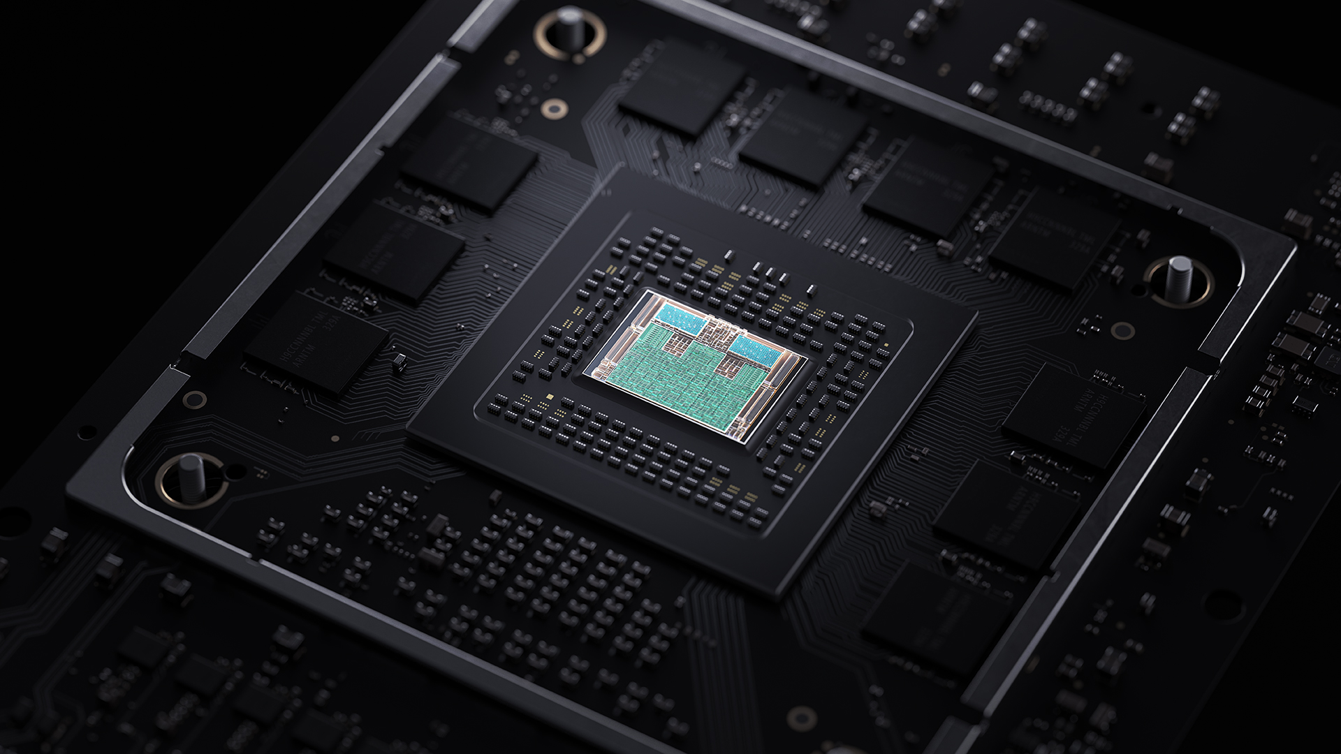
So the XSX has RDNA 2 shader arrays, HW for RT independent of that Shader array, AND special Hardware designed for int/ML work... all concurrent.

All this insight comes directly from Goossen or Fuller who are responsible for the XSX feature set.

I'm not sure where else we can go with this part of the conversation because it seems that our facts are incompatible here..

Your understanding of the featureset is fairly incomplete based what we know today. And there hasn't even been a deep dive as to how it all works together yet.
 
Last edited:

Night.Ninja

Banned
This is how i feel when i come in here

anigif_sub-buzz-25896-1508809027-1.gif


Hands down this is one of the best threads on neo gaf right now

"Without hardware acceleration, this work could have been done in the shaders but would have consumed over 13 TFLOPs alone. For the Xbox Series X, this work is offloaded onto dedicated hardware and the shader can continue to run in parallel with full performance. " In parallel with full performance.

Into integer concurrence:

"We knew that many inference algorithms need only 8-bit and 4-bit integer positions for weights and the math operations involving those weights comprise the bulk of the performance overhead for those algorithms," says Andrew Goossen. "So we added special hardware support for this specific scenario. The result is that Series X offers 49 TOPS for 8-bit integer operations and 97 TOPS for 4-bit integer operations. Note that the weights are integers, so those are TOPS and not TFLOPs. The net result is that Series X offers unparalleled intelligence for machine learning."

Explain this please
 

Ascend

Member
TOPS is tera operations per second. Or trillion operations per second usually denoting integer operations.

This contrasts with tera FLops which is trillions of floating point operations per second.

AI/ML can use either to do inference calculations.
To add to this, the amount of bits is sort of a measure of how precise you can be. The more bits the more precise, and the amount of operations scales proportionally with the amount of bits. So if you have 10 TOPS for 32-bit operations, it would be 20 TOPS for 16-bit, 40 for 8-bit etc.
 

Panajev2001a

GAF's Pleasant Genius


Well, nice of him to confirm that and go on record. The only true thing as others said was the raw bandwidth of the two solutions, 2.4 GB/ and 5.5 GB/s.

The other number/effective compressed bandwidth was the highest technical + marketing + legal was allowed/wanted to quote after as they said after checking internal and external titles. It does not change things from what we were discussing earlier (you can quote 6 GB/s or closer to it, but then for the other console you need to quote something closer to 22 GB/s), but it is nice to hear it repeated.
 
Last edited:

oldergamer

Member
Well, nice of him to confirm that and go on record. The only true thing as others said was the raw bandwidth of the two solutions, 2.4 GB/ and 5.5 GB/s.

The other number/effective compressed bandwidth was the highest technical + marketing + legal was allowed/wanted to quote after as they said after checking internal and external titles. It does not change things from what we were discussing earlier (you can quote 6 GB/s or closer to it, but then for the other console you need to quote something closer to 22 GB/s), but it is nice to hear it repeated.
What would you rate 4.8GB of compressed textures already rejected for what is visible via sfs?
 
Last edited:
Top Bottom