[Digital Foundry]PS5 uncovered

Thanks Digital Foundry for the video.

I guess it was quite hard to create since there is no actual footage of PS5 games to explain the different points you were talking about. I understand what you did with the different cards. 👍👏👍👏👍👏

I can't wait to watch you doing the same video, in the next months, with actual gameplay from the PS5. 😋😉


Digital Foundry also tested

  • RX 5700 super overclock and diminishing frame rate gains due to memory bandwidth limitations.
  • RX 5700 vs RX 5700 XT at the same 9.67 TFLOPS level. RDNA is not GCN.

Even assuming that comparison isn't busted (which it is) doesn't change the fact that SEX bandwidth is about equal to PS5 proportional to computational power.
As far as the comparison its apples to oranges ignoring variables that make it pointless
  • 5700 wasn't designed to clock that high and is power starved at higher frequencies
  • Different architecture
  • RDNA2 is supposed to clock higher
  • The PS5 GPU architecture, silicon design and power delivery was designed around that high frequency which is far different from a PC gamer slapping an aftermarket cooler on a GPU and overclocking it
 
Last edited:
Game was not designed for 8 core cpu's mate. barely any game is. Next gen will peg those CPU's to oblivion specially with increases density of everything AI physics etc. That stuff already was going to happen this generation until devs realized the cpu's simple couldn't handle it for shit. Also big chance that GPU will always sit at 100% usage when dynamic resolution at 4k will push it always to its max.

People can try to sugarcoat the bad design all day long, but what they should do is give sony lots of shit so they can make changes still by redesigning there box to get stable clocks or even go so far to redesign the entire box and slam in the same GPU microsoft has.

GPU barely runs at 100%. It is like saying a car always run's on full power or top speed. Same for the CPU. This time CPU will not be the bottleneck and we should get higher fps but apart from that nothing will change. It depends on the game and it keeps varying on what is happening on screen. GPU is more important for games and we know that little CPU lock speed does not matter much. The bigger problem IMO is RAM. we already have some games using 9-10gigs of GDDR6.
 
Even assuming that comparison isn't busted (which it is) doesn't change the fact that SEX bandwidth is about equal to PS5 proportional to computational power.
As far as the comparison its apples to oranges ignoring variables that make it pointless
  • 5700 wasn't designed to clock that high and is power starved at higher frequencies
  • Different architecture
  • RDNA2 is supposed to clock higher
  • The PS5 GPU architecture, silicon design and power delivery was designed around that high frequency which is far different from a PC gamer slapping an aftermarket cooler on a GPU and overclocking it
https://www.techpowerup.com/review/sapphire-radeon-rx-5700-xt-nitro/33.html
Sapphire Radeon RX 5700 XT Nitro+ already delivers 1971 Mhz average "out-of-the-box" which is 10.09 TFLOPS at 266 watts gaming average.

---

https://www.techpowerup.com/review/msi-radeon-rx-5700-xt-gaming-x/33.html
MSI Radeon RX 5700 XT Gaming X already delivers 1987 Mhz average "out-of-the-box" which is 10,173 TFLOPS at 270 watts gaming average.

---

https://www.techpowerup.com/review/asrock-radeon-rx-5700-xt-taichi-oc-plus/33.html
ASRock Radeon RX 5700 XT Taichi OC+ already delivers 1996 Mhz average "out-of-the-box" which is 10.22 TFLOPS at 274 watts gaming average.

There's more PC AIB RX 5700 XT at near 2Ghz clock speeds "out-of-the-box".

RDNA v1 can reach high clock speeds with relatively high power consumption.

Sony will need AMD's RDNA 2's "50% perf/watt" claimed improvement to reduce RDNA v1's high power consumption at high clock speed.


PC master race can handle +300 watts GPUs.
 
Last edited:
we already have some games using 9-10gigs of GDDR6.
Allocated RAM is not the same as the real usage. 4K does not use more than 6GB of RAM in most titles.

"We often saw VRAM allocation go as high as 8.5 GB when testing with the RTX 2080 Ti at 4K, but there was no performance penalty when using a graphics card with only 6GB of VRAM. There was however a big performance penalty for cards with less than 6 GB.
That is to say, while the game will allocate 8GB of VRAM at 4K when available, it appears to be using somewhere between 4 and 6 GB of memory, probably closer to the upper end of that range."


https://www.techpowerup.com/review/sapphire-radeon-rx-5700-xt-nitro/33.html
Sapphire Radeon RX 5700 XT Nitro+ already delivers 1971 Mhz average "out-of-the-box" which is 10.09 TFLOPS at 266 watts gaming average.

---

https://www.techpowerup.com/review/msi-radeon-rx-5700-xt-gaming-x/33.html
MSI Radeon RX 5700 XT Gaming X already delivers 1987 Mhz average "out-of-the-box" which is 10,173 TFLOPS at 270 watts gaming average.

---

https://www.techpowerup.com/review/asrock-radeon-rx-5700-xt-taichi-oc-plus/33.html
ASRock Radeon RX 5700 XT Taichi OC+ already delivers 1996 Mhz average "out-of-the-box" which is 10.22 TFLOPS at 274 watts gaming average.
Out of the box just means the vendors did a OC on the firmware, its still the same silicon that wasn't designed to clock that high and its still power starved at those frequencies and hitting diminishing returns because of it.
Its no comparison to PS5 or even a off the shelf RDNA2 card, not only is PS5 using RDNA2 (a different architecture that enables higher frequencies) but its also a custom GPU designed around that frequency target on the silicon level and its power delivery optimized around it. Its much more elaborated effort than simply slapping a better cooler on an old architecture card that was never designed to run at those frequencies in the first place.
 
Last edited:
Out of the box just means the vendors did a OC on the firmware, its still the same silicon that wasn't designed to clock that high and its still power starved at those frequencies and hitting diminishing returns because of it.
Its no comparison to PS5 or even a off the shelf RDNA2 card, not only is PS5 using RDNA2 (a different architecture that enables higher frequencies) but its also a custom GPU designed around that frequency target on the silicon level and its power delivery optimized around it. Its much more elaborated effort than slapping a better cooler on an old architecture card that was never designed to run at those frequencies in the first place.
1. Sony acts like PC's AIB GPU board partner on a semi-custom clock speed configuration. The customer relationship is with AIB partner not with AMD.

2. XSX's RDNA 2 scaled to 12.147 TFLOPS which lands on RTX 2080 level results with two weeks raw Gears 5's benchmark with PC Ultra settings indicates near RDNA v1 scaling.

3. RDNA 2 has claimed " 50 perf/watt" improvements and catching up to Turing RTX's hardware feature set.

From https://www.tomsguide.com/news/firs...may-be-revealed-today-with-forza-motorsport-8

Forza Horizon 4
The demo show will reportedly continue with Forza Horizon 4. Here we will see how variable rate shading works on the Xbox Series X. VRS is a technique that allows the GPU to boost detail and quality in complex parts of the images while lowering its power needs in simpler areas.
The reasoning behind VRS is that our eyes and brain can't focus on the totality of an image. If you are paying attention to the screen, your eyes will be focused on where the action is, which typically is the more complex part of the image. The graphics engine doesn't have to spend so much power on the less complex, peripherals parts of the image. That results in power optimization that allows to boost detail even more or increase the frame rate.
The results? Playground Games — who develop the Forza Horizon series — added VRS to Forza Horizon 4 when it received its Xbox Series X development kits in December. That increased the frame rate in the game by a whooping 32% with "no optimizations, just using VRS in parts with motion blur." According to the redditor, "VRS changes the way they design games (VRS as motion blur replacement)," pointing out that the" lead engineer says they can reach 4K/120 today on XSX thanks to RDNA2 architecture and the combined effort of AMD and Microsoft."
Yeah, 4K and 120 frames per second.
Swapping FH4's blur motion into VRS version enables XSX's FH4 to reach 120 fps 4K.

If VRS improves the frame rate by 32 percent which yields 120 fps 4K, then non-VRS version would be 81.6 fps 4K, hence XSX GPU is about 2.72 times better than X1X GPU's FH4 results.

The "no optimizations" could mean running on GCN legacy mode (wave64 instructions) instead of RDNA mode (wave32 instructions)

When running on GCN legacy mode, XSX GPU is effectively ~16.3 TFLOPS GCN.
 
Last edited:
No. The 5700 die is designed to clock high. Reviewers were even surprised at that.

The reason why 5700 clocks not as high as 5700XT, is becaue of lower grade die. Thus even for smaller die, so called narrower but faster, 40CU > 36CU.

Guess which die quality Sony have to pay for, to run 2.23Ghz? :messenger_astonished:

There is a reason why unbiased console warring veterans, are smelling a rat with Mark Sony talks so far....
 
1. Sony acts like PC's AIB GPU board partner on a semi-custom clock speed configuration.

2. XSX's RDNA 2 scaled to 12.147 TFLOPS which lands on RTX 2080 level results with two weeks raw Gears 5's benchmark with PC Ultra settings indicates near RDNA v1 scaling.

3. RDNA 2 has claimed " 50 perf/watt" improvements and catching up to Turing RTX's hardware feature set.
  1. Nope, Sony (like MS) is much more involved in the design processes to the point their collaboration influences RDNA2 design and includes individual customizations, they also get to specify their priorities for the manufacturing process for example frequency over density and design their own power delivery specifically targeting that frequency. AIB vendors get the exact same GPU reference die at most they use higher quality VRMs
  2. Too early to tell, apparently there were different demos making rounds, and it was a quick port
  3. RDNA2 cards will clock higher by default, the microarchitecture is optimized around it and perf/watt improvements are part of that.
No. The 5700 die is designed to clock high. Reviewers were even surprised at that.
Yes, its designed to clock higher than GCN, great improvement on that front
The reason why 5700 clocks not as high as 5700XT, is becaue of lower grade die.
Good point
 
Last edited:
RX 5700 OC/RX 5700 XT equipped PCs have dedicated memory bandwidth allocated to the CPU and audio.


RX 5700 OC to 2150 Mhz yields 9.9‬ TFLOPS

Note that RX 5700 XT (40 CU) has 1887 Mhz average clock speed with 9.66 TFLOPS. From https://www.techpowerup.com/review/amd-radeon-rx-5700-xt/34.html

Again RDNA not sustain 2100Mhz plus it performance not scale proportionally to increase in clock.

Very very misleading.

It is funny the only examples some post here are from RDNA cards at high clock (that are not sustained and bad performance scale) without any clock timeline.

Why not show a comparison with clocks at 1500mhz or so where the clock is stable and performance still is optimal.
 
Last edited:
Allocated RAM is not the same as the real usage. 4K does not use more than 6GB of RAM in most titles.

"We often saw VRAM allocation go as high as 8.5 GB when testing with the RTX 2080 Ti at 4K, but there was no performance penalty when using a graphics card with only 6GB of VRAM. There was however a big performance penalty for cards with less than 6 GB.
That is to say, while the game will allocate 8GB of VRAM at 4K when available, it appears to be using somewhere between 4 and 6 GB of memory, probably closer to the upper end of that range."


It is true that PC comparison can be little misleading as there are so many GPU and CPU and the games never really utilize its potential. Probably Xbox was used as the baseline for dev this gen. But we already knows that for PS4 devs were allowed to use 5.5gigs. According to Microsoft 13.5 will be allowed by them this time. That is barely 2.5 times a leap compared to other components which is massive.
 
  1. Nope, Sony (like MS) is much more involved in the design processes to the point their collaboration influences RDNA2 design and includes individual customization, they also get to specify their priorities for the manufacturing process for example frequency over density and design their own power delivery specifically targeting that frequency. AIB vendors get the exact same GPU reference die at most they use higher quality VRMs
  2. Too early to tell, apparently there were different demos making rounds, and it was a quick port
  3. RDNA2 cards will clock higher by default, the microarchitecture is optimized around it and perf/watt improvements are part of that.
1. RDNA 2 will also benefit PC AIBs when PC's PEG slot and ATX PEG power delivery is spec'ed to 300 watts minimum.

Sony was involved in PS4 Pro's GPU while PC AIB partners raced ahead of AMD's RX 580 (Polaris 20) specs with RX-480 (Polaris 10) silicon.

2. Turing RTX's new hardware features are hardly used with current-gen games. Atm, my RTX 2080 Ti (MSI Gaming X Trio) is acting like a faster GTX 1080 Ti with most current-gen games.

NVIDIA plans to avoid another Kepler.

3. PC's PEG slot and ATX PEG power delivery is spec'ed to 300 watts minimum.
  1. Did i say they wouldn't benefit from RDNA2? no, i said Sony involvement in designing the PS5 GPU is much more deep than AIB vendors who only use reference dies. Sony (and MS) involvement goes as deep as the micro-architecture level and manufacturing of the wafers specifications. Sony had their own launch squedule with with PS4Pro release btw
  2. Im aware of that
  3. Thats great but won't do you any good if the board is not up to par to properly feed the GPU without even taking into account a die core that wasn't mean to clock that high or its of lower grade bin.
 
rdna2 and rdna1 still uses 7nm, so there are limitations already.

MS and sony involvement may help Amd with better efficiency
But to buy a 2.23ghz die with 36.5CU will not be as cheap as it should be.
I see this as a PR forced mistake by Mark. Still trying to talk their way out of it.

MS can just buy the most relaxed 52CU dies and still get away with rolfstomping win.
Phil team wanted this more and took a brave choice on the bigger die.
For the gamers with the best value performing next gen console. :messenger_bicep:
 
Last edited:
rdna2 and rdna1 still uses 7nm, so there are limitations already.
RDNA2 on consoles is using either N7P (DUV) or N7+ both of which are an improvement over N7 used in RDNA
Micro architecture improvements also play a big role remember Kepler->Maswell on the same 28nm process
But to buy a 2.23ghz die with 36.5CU will not be as cheap as it should be.
Depends on how good yields are, smaller die also translates in less defects and more dies per wafer so that definitely helps
 
rdna2 and rdna1 still uses 7nm, so there are limitations already.

MS and sony involvement may help Amd with better efficiency
But to buy a 2.23ghz die with 36.5CU will not be as cheap as it should be.
I see this as a PR forced mistake by Mark. Still trying to talk their way out of it... RDNA uses N7... RDNA 2 uses N7P, N7+ or a mix.

MS can just buy the most relaxed 52CU dies and still get away with rolfstomping win.
Phil team wanted this more and took a brave choice on the bigger die.
For the gamers with the best value performing next gen console. :messenger_bicep:
Just because AMD named N7, N7P and N7+ as 7nm doesn't mean RDNA and RDNA 2 uses the same process.

That is more true when you look at the "50% increase in perf. per watt" that is only possible in a more advanced procesd.

I have a feeling 2.2Ghz for BigNavi will be the norm.
 
Last edited:
  1. Did i say they wouldn't benefit from RDNA2? no, i said Sony involvement in designing the PS5 GPU is much more deep than AIB vendors who only use reference dies. Sony (and MS) involvement goes as deep as the micro-architecture level and manufacturing of the wafers specifications. Sony had their own launch squedule with with PS4Pro release btw
  2. Im aware of that
  3. Thats great but won't do you any good if the board is not up to par to properly feed the GPU without even taking into account a die core that wasn't mean to clock that high or its of lower grade bin.
1. At the end of the day, PC AIB, MS, and Sony are responsible for their shipping product's clock speeds and cooling solutions.

PS4 Pro has launched around November 2016
Ref RX 480 was launched around June 2016.
Non-ref RX 480 was launched around July 2016 e.g.
3. PC AIB RX 5700 XTs out-of-the-box factory OCs are reaching near 2Ghz with ~2Ghz max clock speeds.

The hints for RDNA 2's high clock speed direction is already hinted from non-reference RDNA v1 AIB GPU cards. RDNA 2's "50% perf/watt" improvement is needed to reduce high power consumption at high clock speeds which look silly when compared to Turing RTX.
 
smaller dies dont mean less defect rates since the 40CU is separate from the 58CU part.

I predict the 6700XT can run comfortably at 2Ghz. But for Sony, they need to buy the lower grade 6700, with 36.5CU that runs at 2.23ghz, not cheap.
 
1. At the end of the day, PC AIB, MS, and Sony are responsible for their shipping product's clock speeds and cooling solutions.

PS4 Pro has launched around November 2016
Ref RX 480 was launched around June 2016.
Non-ref RX 480 was launched around July 2016 e.g.
3. PC AIB RX 5700 XTs out-of-the-box factory OCs are reaching near 2Ghz with ~2Ghz max clock speeds.

The hints for RDNA 2's high clock speed direction is already hinted from non-reference RDNA v1 AIB GPU cards. RDNA 2's "50% perf/watt" improvement is needed to reduce high power consumption at high clock speeds which look silly when compared to Turing RTX.
  1. At the end of the day Sony & MS use custom dies designed around a specific frequency sweet spot. AIBs use the same reference dies that's why its called an overclock.
  2. Again PS4Pro had its own launch schedule and logistics, discrete cards release dates are irrelevant
  3. Yes they are overclocked and hitting disminishing returns. Console chips aren't overclocked, they were designed around that target
 
smaller dies dont mean less defect rates since the 40CU is separate from the 58CU part.
What that even means?

Smaller die = more chip per wafer.
So even if the defect rate is the same you still has way more good chips... and cheaper.

But most cases big dies have more defectives because it take a bigger area in the wafer.
 
smaller dies dont mean less defect rates since the 40CU is separate from the 58CU part.

I predict the 6700XT can run comfortably at 2Ghz. But for Sony, they need to buy the lower grade 6700, with 36.5CU that runs at 2.23ghz, not cheap.

Sony is getting an unreleased RDNA2 based semi custom design not buying something from the store and over clocking it.
 
smaller dies dont mean less defect rates since the 40CU is separate from the 58CU part.

I predict the 6700XT can run comfortably at 2Ghz. But for Sony, they need to buy the lower grade 6700, with 36.5CU that runs at 2.23ghz, not cheap.
Yes that's exactly how it works, the bigger the die the more chances for defects. Bigger also translates into less dies per wafer
You are assuming Sony will use an off the shelf gpu die when in reality they have their own custom apu die with their own manufacturing specifications, every single die from the wafer goes to them.
 
Last edited:
What that even means?

Smaller die = more chip per wafer.
So even if the defect rate is the same you still has way more good chips... and cheaper.

But most cases big dies have more defectives because it take a bigger area in the wafer.

Let me google for dies defect rates, should i have the time.
The point is, in normal case, bigger die design is more expensive. Be it from defect rates or lesser dies. Ok.
But Sony had to buy 'un-normal' dies, the intended savings are questioned by us.

Sony is getting an unreleased RDNA2 based semi custom design not buying something from the store and over clocking it.

Sony still have obey physical limitations, semi custom or not.
Unless perhaps, to force the 2.23ghz, they semi-dropped features of Rdna2, like vrs, full hw RT...:eek:
 
While the xbox is more powerful than PS5, I have to ask so what ? xbox 1 was more powerful ps2. Xbox360 was better than PS3 in multiplatform games. PS4 pro is way less powerful in every possible way compared to the one X.

the percentage difference between series X and PS5 is less than PS4 pro and one X, YET that didnt save the console to be first place .

it will always. ALWAYS ( repeat after me , ALWAYS ) come to the exclusive games.

and till MS start delivering high quality AAA games, they will always lose ( and I no longer even own a ps4 pro because of the horrible jet engine sound i switched to xbox one X scorpio edition )

personally i do like Halo and forza, and i do like sony offering too. but i am not a majority. MS needs to address their first party line up for big AAA games not just AA games in a short period of time netflix style ( which is sadly is what they are aiming for at least for the majority of their studios while few other studios focus on AAA games )

mean while at Sony its one hit after the other.
 
rdna2 and rdna1 still uses 7nm, so there are limitations already.

MS and sony involvement may help Amd with better efficiency
But to buy a 2.23ghz die with 36.5CU will not be as cheap as it should be.
I see this as a PR forced mistake by Mark. Still trying to talk their way out of it.

MS can just buy the most relaxed 52CU dies and still get away with rolfstomping win.
Phil team wanted this more and took a brave choice on the bigger die.
For the gamers with the best value performing next gen console. :messenger_bicep:

36.5 CU die?!? Relaxed 52 CU's @1.8 GHz die?!? ... and the marketing headline at the end :LOL:. You are excited, I get that :).
 
  1. At the end of the day Sony & MS use custom dies designed around a specific frequency sweet spot. AIBs use the same reference dies that's why its called an overclock.
  2. Again PS4Pro had its own launch schedule and logistics, discrete cards release dates are irrelevant
  3. Yes they are overclocked and hitting disminishing returns. Console chips aren't overclocked, they were designed around that target
1. Sony obeys the same laws of physics as any other PC AIB vendor.
2. That's not the argument.
3. Sony obeys the same laws of physics as any other PC AIB vendor.
 
Last edited:
I'm just waiting to see what the cooling solution is like for PS5. I'm not going to get too involved with all the crazy speculation, but I still personally think that "variable frequency" was brought up originally to be able to tout max performance numbers - and I also think that thermal throttling is still a thing (it is). I hope they really surprise me with their cooling solution.
 
Sony still have obey physical limitations, semi custom or not.
Unless perhaps, to force the 2.23ghz, they semi-dropped features of Rdna2, like vrs, full hw RT...:eek:

... what kind of person would be so sure that the design is not capable of that high boost frequency as they optimised the chip's layout and manufacturing process to get there (well aware of the limitations of physics there)? Well, given your comment about RT again I think you already answered ;).
 
1. Sony obeys the same laws of physics as any other PC AIB vendor.
2. That's not the argument.
3. Sony obeys the same laws of physics as any other PC AIB vendor.

Sure, but PC AIB vendors are not in control of the entire system design and cooling ( did not they customised the final chip with AMD around that either) nor are currently using either the XSX or PS5 chips as they have yet to be released.
 
36.5 CU die?!? Relaxed 52 CU's @1.8 GHz die?!? ... and the marketing headline at the end :LOL:. You are excited, I get that :).

I believe Sony just repurposed one of the dead CU into their Tempest chip. Hence 36.5CU.
Either that or Amd does another of their Truaudio tensilica core thing, which means Series X likely to have the same thing in their APU. If so, it is a yawn for MS to hype on it.

52CU at 1.8ghz is probably the base line for Amd next gen 6800 GPU.
Their first 7nm 60CU gpu Radeon7 already runs comfortably at 1.75ghz.
 
Last edited:
1. Sony obeys the same laws of physics as any other PC AIB vendor.
2. That's not the argument.
3. Sony obeys the same laws of physics as any other PC AIB vendor.
  1. AIB vendors are not involved on the micro architecture design, they just buy a reference die hence why they overclock over the reference values. Sony is involved in the design of their custom die made around their specifications, they don't overclock their capped frequency is the reference value sweet spot the silicon was designed for
  2. You gave me no argument, just threw random release dates out of context
  3. Sony can set their own priorities on the micro architecture level and manufacturing process (prioritize frequency over density)
 
I believe Sony just repurposed one of the dead CU into their Tempest chip. Hence 36.5CU.
Either that or Amd does another of their Truaudio tensilica core thing, which means Series X likely to have the same thing in their APU. If so, it is a yawn for MS to hype on it.

52CU at 1.8ghz is probably the base line for Amd next gen 6800 GPU.
Their first 7nm gpu Radeon7 already runs comfortably at 1.75ghz.
They are probably not using one of the GPU dead CUs. Sony modified the CU, removed the cache and probably did others modifications, they can't predict which CUs are going to be deactivated.

Also they can't predict that at least one deactivated CU should not have any defect in order to be used as the Tempest CU.
 
Last edited:
They are probably not using of the GPU dead CUs. Sony modified the CU, removed the cache and probably did others modifications, they can't predict which CUs are going to be deactivated.

By dead, i am thinking for full gpu purpose. Sony just found enough use to recycle one for audio, hence the 'stripping' parts and it running at the same 2.23ghz freq and taking the same memory bandwith.
So they can 'predict' this dead CU, 36.5CU is probably generous to call. Maybe a 36.25CU part. :messenger_astonished:
 
But Sony had to buy 'un-normal' dies,
How do you even know what's normal or base clocks for RDNA2? For all we know PS5 clocks are normal for a chip that size.
Sony just found enough use to recycle one for audio
"recycling" a CU would defeat the purpose of disabling them for yields
The audio silicon uses a CU as its basis but it redesigned taking what they learned from SPUs to more effectively & efficiently process audio. The 4 extra disabled CUs are still there
 
  1. AIB vendors are not involved on the micro architecture design, they just buy a reference die hence why they overclock over the reference values. Sony is involved in the design of their custom die made around their specifications, they don't overclock their capped frequency is the reference value sweet spot the silicon was designed for
  2. You gave me no argument, just threw random release dates out of context
  3. Sony can set their own priorities on the micro architecture level and manufacturing process (prioritize frequency over density)
1. Against "AIB vendors are not involved on the microarchitecture design". Not my argument.

Against "they just buy a reference die hence why they overclock over the reference values", Again, at the end of the day, MS, Sony, and PC AIBs are responsible for placing clock speed settings and cooling solutions on their shipping product.

My MSI R9-290X Gaming X OC still works and it was ahead of AMD's R9-390X reference with a tiny 10 Mhz clock speed difference LOL. Your "overclock" = bad argument is fluff.

2. Your argument is fluff. i.e. your "Sony is involved in the design of their custom die made around their specifications " has resulted in PS4 Pro's sub-par Polaris kitbash! Sony still has to obey the laws of physics.

3. Your "Sony can set their own priorities on the microarchitecture level and manufacturing process" is another fluff i.e. not my argument. Sony still has to obey the laws of physics.
 
They are probably not using one of the GPU dead CUs. Sony modified the CU, removed the cache and probably did others modifications, they can't predict which CUs are going to be deactivated.

Also they can't predict that at least one deactivated CU should not have any defect in order to be used as the Tempest CU.
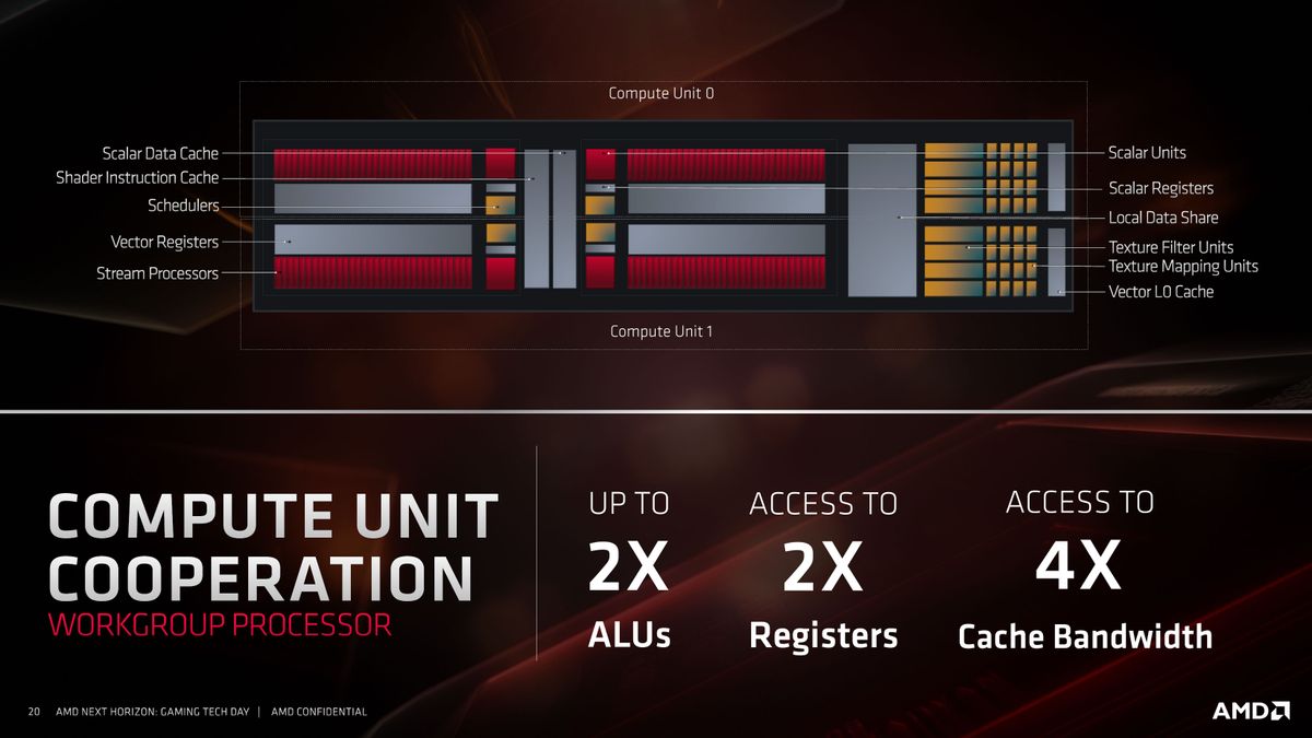
RDNA CU already has LDS (Local Data Store) and texture fetch, texture mapping, texture filter, and 'etc'. Cutting out graphics hardware saves on transistor count.

T76hJFXMy7JvEqbYMP5huf-1200-80.jpg
 
1. Sony acts like PC's AIB GPU board partner on a semi-custom clock speed configuration. The customer relationship is with AIB partner not with AMD.
"Sony can set their own priorities on the microarchitecture level and manufacturing process" is another fluff i.e. not my argument
1. Against "AIB vendors are not involved on the microarchitecture design". Not my argument.
🤔 🤥
Again, at the end of the day, MS, Sony, and PC AIBs are responsible for placing clock speed settings and cooling solutions on their shipping product.
Again AIBs overclock over reference values, console chips capped frequencies are the reference values, thats the difference
Your "overclock" = bad
Never said that
 
Last edited:
PS 5 seems like a Saturn; underpowered GPU but faster load times and a crazy powerful Sound system.

Both the Series X and PS5 will be great mind
 
Last edited:
Sure, but PC AIB vendors are not in control of the entire system design and cooling ( did not they customised the final chip with AMD around that either) nor are currently using either the XSX or PS5 chips as they have yet to be released.
Your arguments are similar to when Mark Cerny harp on "supercharge PC and special customizations for PS4" when R9 290X was released around October 2013 ahead of PS4 and obliterated the "supercharge PC".

October 2020 is for PC's RDNA 2.
 
I still don't understand this whole yields thing with the CUs.

So, the XSX has 56 CUs, but 4 of them are disabled, hence 52.

But why are 4 of them disabled? How does that help yields? Why can't you get 56 fully operational CUs?

Someone ELI5.
 
Your arguments are similar to when Mark Cerny harp on "supercharge PC and special customizations for PS4" when R9 290X was released around October 2013 ahead of PS4 and obliterated the "supercharge PC".

October 2020 is for PC's RDNA 2.

Obliterated :LOL: ? Consoles have a lead time to hit the launch date with millions of units while on PC you tend to paper launch and slowly increase availability so of course PS4 had to lock things earlier and co-designed customisations hit on PC too at a later date. But sure, Cerny "harps on" :rolleyes:.
 
🤔 🤥

Again AIBs overclock over reference values, console chips capped frequencies are the reference values, thats the difference

Never said that
FYI, PS4 Pro GPU's 911 Mhz is not a reference clock speed for RX-470's 926 Mhz base with 1206 Mhz boost.

Again, Sony is responsible for PS4 Pro's GPU clock speed and cooling solution like any other PC AIB.
 
I still don't understand this whole yields thing with the CUs.

So, the XSX has 56 CUs, but 4 of them are disabled, hence 52.

But why are 4 of them disabled? How does that help yields? Why can't you get 56 fully operational CUs?

Someone ELI5.
Under RDNA design, two CUs are closely linked together to form "DCU". Disable two DCU = four CU disabled in GCN speak.
 
Again RDNA not sustain 2100Mhz plus it performance not scale proportionally to increase in clock.

Very very misleading.

It is funny the only examples some post here are from RDNA cards at high clock (that are not sustained and bad performance scale) without any clock timeline.

Why not show a comparison with clocks at 1500mhz or so where the clock is stable and performance still is optimal.
1. My Techpowerup links have average clock speed statistics.
2. PC RX 5700 XT's 448 GB/s bandwidth is not being shared with audio and CPU.
 
FYI, PS4 Pro GPU's 911 Mhz is not a reference clock speed for RX-470's 926 Mhz base with 1206 Mhz boost.

Again, Sony is responsible for PS4 Pro's GPU clock speed and cooling solution like any other PC AIB.
FYI the Pro isn't using a off the shelf card, they they have their own custom design with specific targets
Again, AIBs buy stock reference dies and overclock over reference values, AMD works with sony to design the SoC around their targets, console chips capped frequencies are the reference values.
 
Last edited:
But for Sony, they need to buy the lower grade 6700, with 36.5CU that runs at 2.23ghz, not cheap.
Pack it up Sony. Your scam of hacking together cheap RDNA1 off-the-shelf parts (that end up not being cheap) has been exposed. :pie_roffles:

Edit: amazing, some even thought I was serious.
 
Last edited:
rdna2 and rdna1 still uses 7nm, so there are limitations already.

MS and sony involvement may help Amd with better efficiency
But to buy a 2.23ghz die with 36.5CU will not be as cheap as it should be.
I see this as a PR forced mistake by Mark. Still trying to talk their way out of it.

MS can just buy the most relaxed 52CU dies and still get away with rolfstomping win.
Phil team wanted this more and took a brave choice on the bigger die.
For the gamers with the best value performing next gen console. :messenger_bicep:

Dont feed the trolls kids, schools out.

 
Last edited:
Top Bottom