Sinthor
Gold Member
The NVME 4 spec is capable of supporting up to 7Gb/s transfer rates so there's no limit being hit using 4 lanes for either Sony or MS.
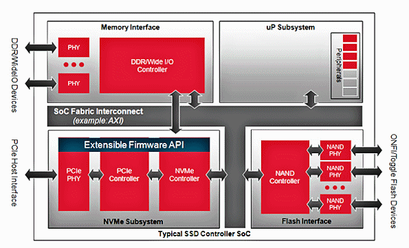
For the NAND storage, Sony and MS will be buying commercially available quality from whichever memory partners they're working with. Speed improvements will come from how they've specced the NAND/SSD they're using coupled with what they can do with cusom controllers and firmware. I'm assuming both compaines are using a commercially available SSD as the basis for their solution. MS just chose one and put it in their system with little customisation, Sony chose one and have taken it apart to install their own channel architecture and controller to boost the access times.
What happens "inside" the SSD - that's between the controller and the NANDs - is where the speed gain is made. 12 vs 8 channels is one way to boost access times.
Then there's the type of NAND being used - SLC, MLC, TLC. SLC is fastest offering read speeds less than half that of TLC and it's more resistant to high thermal outputs. SLC is also more expensive and perhaps beyond Sony's budget. MLC is about 1/3rd faster than TLC and not so expensive. Maybe Sony went that way and MS used TLC NAND - this plus 12 channels would account for the latency difference.
It could be Sony are just brute forcing it -they went with TLC, 12 channels and then bumped the clock rates on the SSD and installed heavy cooling so it can run at those speeds. This would map on to the issues around CPU/GPU power consumption, variable clock speeds and allocating power dynamically. I don't think Sony has done that but until we see the PS5 we won't know for sure.
Aha! I see it now. Thank you very much for the explanation! I'm back on the "I get this!" train!
")


 ❤
❤