Gonzalo was tested as recently as august pr september, maybe even later. If we believe AquariusZ or whatever his name is, he himself is very surprised that oberon is still undergoing testing if it's supposed to launch next november.
I'm one of the few that does believe there is some merit to the ps5 originally being scheduled for 2019. NAVI being a year late is probably the reason the change to 2020 happened. If you look at amd slides from 2015/2016, navi is listed as a 2018 release. but it ended up coming in july 2019. If the rumor of the 2019 plan being scrapped in 2017 is true, does that give sony enough time and incentive to scrap the chip design they've poured millions into or do they try to wring out as much power as possible out of what they've been working on? The fact they've steadily upped the quality of memory chips from ariel to oberon could mean that is what they're trying to do. Increase bandwidth to make up some of the perceived lack in power. In 2017 the chip would've been a year away from being finalized for a 2019 release.
Apisak did say that that fake code names have popped up, sure, but there's nothing to show just how far back that deception started. We do know that AMD code name decoder changed with zen 2 IIRC. So it could go as far back as that.
This is all speculation of course. Just saying what makes sense to my ignorant little mind.
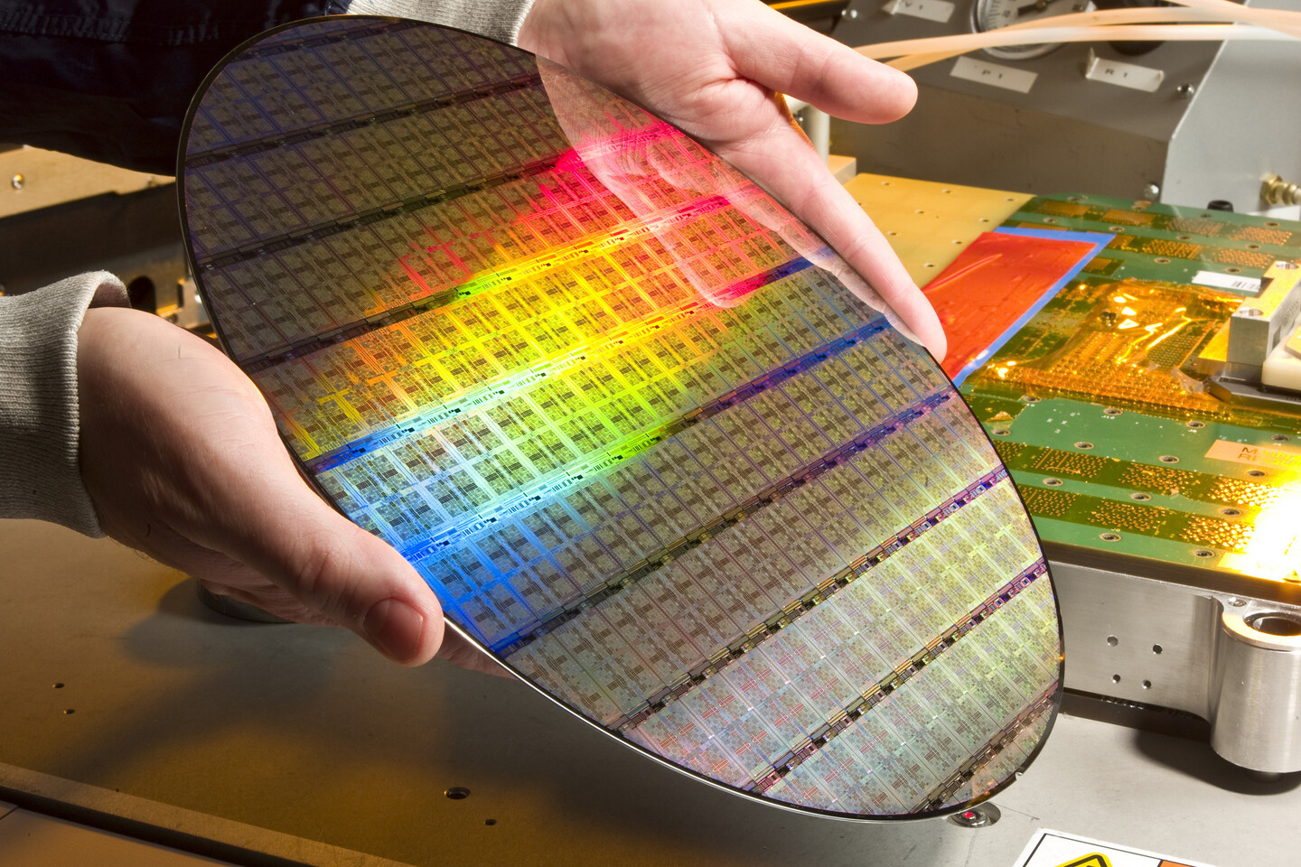
Prices are going up as early as this quarter for NAND/ssds. The demand for consoles is probably a part of the reason.
According to the sources over at DigiTimes, NAND flash prices are set to rise by up to 40% in 2020. This report is coming from sources over at memory chipmakers, presumably some of the biggest players like SK Hynix, Micron, and Samsung. If the prediction realizes, consumers will see a...

www.techpowerup.com