-
Hey Guest. Check out your NeoGAF Wrapped 2025 results here!
You are using an out of date browser. It may not display this or other websites correctly.
You should upgrade or use an alternative browser.
You should upgrade or use an alternative browser.
- Status
- Not open for further replies.
secondo me ps5 e dual gpu chipled con il raytracing separato dalle gpu connesso in parellelo alle gpu .
perche dual gpu ? per gestire meglio i 2 segnali video per il psvr2 le 2 gpu possono renderizzare in vr2 redering separati
perché Sony dovrebbe concentrarsi troppo su VR2?
dual gpu puo essere terribile in ambito pc ma in un hardware chiuso ottimizzato creando bus di collegamento piu veloci delle pci express e tutta unaltra storia
per quanto riguarda il sistema di raffreddamento nn e cosi difficile proggettarlo basta fare consol a sendwich dissipatore che occuba la parte sotto e sopra le periferiche
nn e che ci va uno scenziato termico e poi fatto in alluminio nn costerebbe manco tanto anche perche lefficenza di un dissipatore in alluminio nn e secondo a nessuno con la ventola messa in mezzo tipo ps3 risolvi tutto
Please translate to English before posting going forward. Thank you.
James Sawyer Ford
Banned
Well, both can still adjust clock and mem size.
Would it be too crazy to think Oberon is just a PS4 Pro revision using zen2+navi?
yes but you can still announce minimum clock and mem targets without tipping your hand on the final configuration
at this stage memory quantities are locked down, contracts in place
I realistically only see minor clock adjustments being the last piece
A few people have asked me about raytracing now, so I thought I would enquire at our latest drinking session. There isn't a lot I can tell you right now. But what I can say is when turning on raytracing in engine on PS5 devkit the frame rate cost is around 30%. Bearing in mind this is before any optimisation. The Dev team think they will be able to get this down to 15-20%, which should be enough to hit their target frame rate without too much trouble. On the PC turning on the same effects on Nvidia hardware costs around 35%. I can't give you comparison with Series X as the team are still yet to receive their kits. Apparently they may have to wait till April! Which would give Sony a considerable leg-up in terms of hands on time with the hardware. This may also explain why no Series X exclusives for launch, if teams simply haven't had long enough to aquiant themselves to the hardware.
Hi there. Please check your PMs on the process before posting as a developer or inside knowledge.
TLZ
Banned
Very excited for these new systems. When I was growing up, my Dad was a small-town doctor for over 50 years and he didn't much play games(though being a military man, he'd make you look inept at Duck Hunt), but he loved to see the way they advanced over the years and encouraged the hobby, much as I do with my son now.
I remember purchasing my PS3 and he was blown away by Blu-Ray at the time.
His passion was audio equipment and music(instrumental) and he would often buy soundtracks to many of my games once they progressed beyond the bleeps and blips of consoles past.
Man, if he was around to see what these new systems would be able to do coming up.

liviopangt
Neo Member
do you sincerely believe that ps5 has only 36 cu? if it were to recover the disadvantage they should implement a raytracing engine twice as big as xsx to not stress more than 5 -10% the gpu?yes but you can still announce minimum clock and mem targets without tipping your hand on the final configuration
at this stage memory quantities are locked down, contracts in place
I realistically only see minor clock adjustments being the last piece
James Sawyer Ford
Banned
do you sincerely believe that ps5 has only 36 cu? if it were to recover the disadvantage they should implement a raytracing engine twice as big as xsx to not stress more than 5 -10% the gpu?
no, I think it has 54 CU
JLB
Banned
No, I don't own any consoles, I've never played a game before. I certainly don't own all of them, including the bastard vita. I have no idea what I'm talking about, it's not like I spent the last twenty bloody years making games.
Indeed looks like that.
darkinstinct
...lacks reading comprehension.
however if sony nn has still released the full specifications and because they don't want microsoft engineers to bring improvements at the last minute to the gpu and ram everything will be revealed as soon as the games are done and the chips in production
I doubt that's the reason for secrecy. They have to know that Microsoft could just as easily clock their APU at 2 GHz to reach 14.34 TF. That's what the XSX design allows, maximum cooling. They don't want to go there because of power consumption - but that would be a very simple change that they could implement even in August 2020 for a holiday launch. They did something similar with Xbox One. But there is one very good reason for being quiet: If you would know that you had the weaker system. Because if Sony comes out now and says "Hey, here is our 9.2 TF console" they will lose all momentum. So they will probably not talk about specs at all if that is indeed the case.
I think they are taking two very different approaches. Microsoft is building an absolute power machine. It will probably sell less than 15 million units lifetime. Sony is building a console that is going to sell 150 million units. Microsoft has a second SKU that will do the grunt work. XSS will sell many, many more units than XSX.
Last edited:
SmokSmog
Member
54CUs at 2GHZ ?

40CUs stock (dynamic clock 1800-2000mhz). GPU Only!
source https://www.tomshardware.com/reviews/amd-radeon-rx_5700-rx_5700_xt,6216-5.html
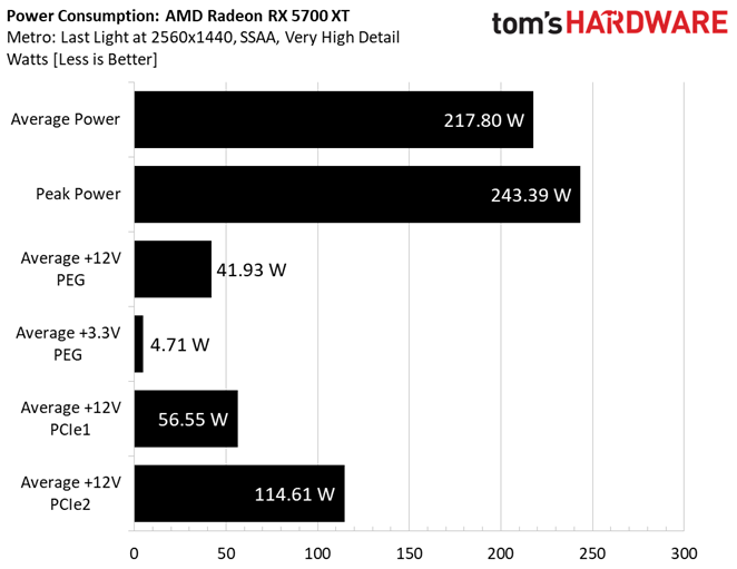
40CUs stock (dynamic clock 1800-2000mhz). GPU Only!
source https://www.tomshardware.com/reviews/amd-radeon-rx_5700-rx_5700_xt,6216-5.html
Did a few test runs today with my 5700XT reference design in Shadow of the tomb raider with different voltagesettings etc. Tested with TAA, dx12 and highest in 1080p. Custom fancurve. Temps are maxtemps.
Stock 2050/1200mv:
110fps, 185W max, 160W avg, rpm 2950, gputemp 74C, junction 93C
1900MHz/1000mv:
110fps, 149W max, 130W avg, rpm 2700, gputemp 70C, junction 81C.
1800/950mv:
108fps, 133W max, 115W avg, rpm 2300, gputemp 66C, junction 74C.
1750/910mv:
106fps, 134W max, 110W avg, rpm 2300, gputemp 66C, junction 74C.
1700/890mv:
104fps, 126W max, 105W avg, rpm 2200, gputemp 65C, junction 73C.
Conclusion:
Underclock to 1900 and UV to 1000mv gives no performanceloss, but temps are better and slightly less noise.
Underclock to 1800 only gives 3% performanceloss, but reduces powerusage by 10-15% and temps quite a bit.
Underclocking/undervolting further yields 5% lower power pr 2% performance and is not worth it in my opinion.
Seems like 1800/950mv is the sweetspot 8n my card
Reactions:Schmuckley, potato580+, Apocalypsee and 16 others
Last edited:
David Ricardo
Member
Maybe you could change it to "I don't think Sony needs to be so secretive and ambiguous".No, I want to say that, personally, I don't think Sony needs to get away with so much secrecy and ambiguity.
Don't know if I translete it correctly.
No, quiero decir que, personamente, no creo que Sony tenga necesidad de andarse con tanto secretismo y ambigüedad.
Sounds like you think Sony specs are good.
bitbydeath
Gold Member
And? That's a silly reason to consider the whole thing a conspiracy theory. These are mega-conglomerates; they have their hands in a LOT of ventures, same goes for Sony. And a venture having ownership held by a given company does not mean that venture works on behalf of it's owning corporate shareholder on something as petty as console spec FUD.
Just keep in mind most people who lend credibility to the Github leak aren't doing it out of spite or even because they think those are PS5's (or XSX's for that matter) final specifications. However, while it's completely ridiculous there are folks who think the Github stuff tells 100% of the story, it's just as ridiculous there are people trying to say it tells literally 0% of the story, as well. It's relevance is pertinent, but it's still just a segment of the whole picture.
TL,DR; people on both sides need to stop taking such polarizing, extreme stances on the issue.
So that screenshot had nothing to do with Github. Google Drive is not Github related in anyway shape or form.
darkinstinct
...lacks reading comprehension.
Those were takedown notices because somebody copied the info to their Google Drive.So that screenshot had nothing to do with Github. Google Drive is not Github related in anyway shape or form.
Classicrockfan
Banned
What in the haberdashery and hemoglobin is going on here?
Tarkus98
Member
The thing I don't understand is the rumor that Sony was going to launch in 2019. If they had an 8 or 9 Tflop console ready for last year then why didn't they launch it? Get a year jump on Microsoft's console and run up the sales. Why hold off a year and release basically the same 9 Tflop console (perhaps with a few more tweaks) and look weak compared to Microsoft's offering? Does not compute.
Neo Blaster
Member
Well, 54 fits that butterfly design they used on the pro for native BC:no, I think it has 54 CU
PS4: 18
PS4 Pro: 36(18 disabled for PS4 BC mode)
PS5: 54(18 disabled for PS4 Pro BC, 36 disabled for PS4 BC)
bitbydeath
Gold Member
Those were takedown notices because somebody copied the info to their Google Drive.
Who copied it to their Google Drive? We've never seen links to that here?
Edit: Where's the link that states it is github file related? When we don't know what was on a random google drive?
Last edited:
desennium
Neo Member
What in the haberdashery and hemoglobin is going on here?
... a Tony Baker fan i see!
")
DeepEnigma
Gold Member
FOURTEEN POINT TWO TERROR FLOPPIES.
Excuse me, I'm just about to go take a hammer to my 2080ti For being so underpowered and so expensive compared to the almighty PlayStation. Hail hydra.
Wait didn't some of you tits say just recently that Ms couldn't possibly have anything as high as over 12tf because it wouldn't work due to heat/power/cockroaches...?
Make up your damn minds people
Bruh, dial it right back down a bit.
Don't be angry because you pay nVidia tax.

chilichote
Member
No, I want to say that, personally, I don't think Sony needs to get away with so much secrecy and ambiguity.
Don't know if I translete it correctly.
No, quiero decir que, personamente, no creo que Sony tenga necesidad de andarse con tanto secretismo y ambigüedad.
Do you mean:
No, I want to say that personally I don't think Sony has to be so mysterious and ambiguous.
Roronoa Zoro
Gold Member
What about taller and/or deeper? Would those help? I always liked how WiiU used that behind the console space that is usually wastedSony can go narrow and 8-9.5TF or wide 11-13TF there is no other option. You can make 36-40cus at 2GHZ but it will be very inefficient.
Imagine ps5 9TF consuming the same amount of power as 12TF XSX.
SmokSmog
Member
What about taller and/or deeper? Would those help? I always liked how WiiU used that behind the console space that is usually wasted

chilichote
Member
If Sony had launched in 2019, the PS5 would have had 36 CUs. It makes no sense to move the console a year and then launch with the same amount of CUs.
Unless there are two SKUs, a normal PS5 and a PS5 Pro.
Unless there are two SKUs, a normal PS5 and a PS5 Pro.
Last edited:
Aressa
You can't die before your death
What in the haberdashery and hemoglobin is going on here?
What in the duel GPU is happing here?
darkinstinct
...lacks reading comprehension.
Except for the fact that Oberon is clearly Navi10 according to the leak and thus can't be more than 40 CU. You can't take just parts of the leak. If you believe that they were testing BC for PS5, then it's a Navi10 APU with a max of 40 CU. If you don't believe they were testing that at all it could be a 54 CU chip based on Navi21.Well, 54 fits that butterfly design they used on the pro for native BC:
PS4: 18
PS4 Pro: 36(18 disabled for PS4 BC mode)
PS5: 54(18 disabled for PS4 Pro BC, 36 disabled for PS4 BC)
BGs
Industry Professional
(Thanks about the translation)Maybe you could change it to "I don't think Sony needs to be so secretive and ambiguous".
Sounds like you think Sony specs are good.
Sounds like Sony specs are "irrelevant".
darkinstinct
...lacks reading comprehension.
Of course it makes sense. A completely new APU design back in March 2019 would set them back two years. So that would lead to a 2021 launch. Modifying an existing APU results in six to 12 months delay, which is exactly what they would've needed. Note that Cerny said in April 2019 that they were using a low powered version of the PS5 APU in their devkits - back then Oberon didn't exist. Oberon is the high power final version that they used to replace their low power Ariel devkit with.If Sony had launched in 2019, the PS5 would have had 36 CUs. It makes no sense to move the console a year and then start with the same amount of CUs.
Unless there are two SKUs, a normal PS5 and a PS5 Pro.
chilichote
Member
Sounds like Sony specs are "irrelevant".
What does that mean?
Mriverz
Member
<blockquote class="twitter-tweet">
I'm sorry you all have to wait a bit longer for the #PlayStation5 reveal, but I have this bet going on that I wouldn't dare skipping all of February without giving even a date.
Watch me pull it off, @XboxP3, those 100 Dollars are mine!
— Jim Ryan SIE - almost authentic (@JimRyanSIE) February 6, 2020
Messed that up lol but ya on his Twitter
#Bringbacklayden!!
Last edited:
chilichote
Member
Of course it makes sense. A completely new APU design back in March 2019 would set them back two years. So that would lead to a 2021 launch. Modifying an existing APU results in six to 12 months delay, which is exactly what they would've needed. Note that Cerny said in April 2019 that they were using a low powered version of the PS5 APU in their devkits - back then Oberon didn't exist. Oberon is the high power final version that they used to replace their low power Ariel devkit with.
What do you think they changed?
RDNA, 7nm, 36 CUs are identical.
Apart from the clock rate and a few tweaks, there is not much to get out of it. Especially considering that Microsoft is very likely to start with more than 36CUs in 2020. So Sony would have lost a year ahead. And the chance to conter the XseX in 2020 with a pro. So it's just a design that was meant for 2019 with a few tweaks.
DJ12
Member
Kaz CEO wannabe without the charm and humour lol<blockquote class="twitter-tweet">
I'm sorry you all have to wait a bit longer for the #PlayStation5 reveal, but I have this bet going on that I wouldn't dare skipping all of February without giving even a date.
Watch me pull it off, @XboxP3, those 100 Dollars are mine!
— Jim Ryan SIE - almost authentic (@JimRyanSIE) February 6, 2020
Messed that up lol but ya on his Twitter
#Bringbacklayden!!
SlimySnake
Flashless at the Golden Globes
so you are saying the ps5 will have a 243w gpu, plus 50w for cpu and another 50 watts for ram, ssd and other stuff on the motherboard?54CUs at 2GHZ ?
40CUs stock (dynamic clock 1800-2000mhz). GPU Only!
source https://www.tomshardware.com/reviews/amd-radeon-rx_5700-rx_5700_xt,6216-5.html
so a 350w console? just to save a few dollars on a bigger die with 20 more CUs?
Fake
Member
hmm did ariel leak mention the cpu ? there was roumer about next gen console will be using jaguar cpuWhat do you think they changed?
RDNA, 7nm, 36 CUs are identical.
Apart from the clock rate and a few tweaks, there is not much to get out of it. Especially considering that Microsoft is very likely to start with more than 36CUs in 2020. So Sony would have lost a year ahead. And the chance to conter the XseX in 2020 with a pro. So it's just a design that was meant for 2019 with a few tweaks.
also it could be bugs in devkit and i think the BW was slower in ariel
darkinstinct
...lacks reading comprehension.
What do you think they changed?
RDNA, 7nm, 36 CUs are identical.
Apart from the clock rate and a few tweaks, there is not much to get out of it. Especially considering that Microsoft is very likely to start with more than 36CUs in 2020. So Sony would have lost a year ahead. And the chance to conter the XseX in 2020 with a pro. So it's just a design that was meant for 2019 with a few tweaks.
They changed the clockspeeds and added hardware raytracing (though probably not from AMD, because that requires Navi21, they could use LocalRay). It's even possible that they had to raise the clockspeeds because of raytracing, to mitigate the performance impact. Why would they enter an arms race when as you correctly say they can launch a Pro in 2021 or 2022? They will probably have a cheaper console than XSX in 2020 and then in two years they will have their own 499 SKU that is more powerful than XSX while PS5 and XSX drop to 299 and 399. And then in 2024 Microsoft goes to 3nm and does their ... Series X X. LOL. It really doesn't matter to be the most powerful, in fact the most powerful has almost never one its generation. Even this gen the Switch could end up being the winner. Price/performance is the important part, games are important.
Looking a the V shaped design – which is iconic like the launch ps1, ps2, p3 designs (IMHO), so possibly the real shape – it would suggest cooling symmetry beyond cooling symmetrical memory layout.
I'm now thinking the Github leak is real for PS5, but for Sony to again play to their EE design strengths (like Ps2, PS3 and Ps4) they are going to use Dual Oberon chips and downclock at whatever level they can, to beat MS using a single RDNA2 XsX chip (with them rebinning defects as XsS).
A dual chip setup for PS5 would allow them to hit much higher performance – like their PS2 Dual coprocessor design and intended PS3 dual Cell processor design. They would also maximize their waffer yield and could aim lower power and quieter if downclocking heavily to hit 7TF from each. A solution like this might also explain why someone mentioned they are still negotiating price with AMD, and why general consensus of their SSD solution being faster and them being better on the RT side of things, and suggestions they might be above RTX 2080 TI. I know it is wishful thinking
I also think the 3D audio chip inside the APU is an AMD version of the Cell processor, making BC completely doable in hardware, but that's more wishful thinking by me, I suspect
Yeah, I'm in the camp that it's not set in stone yet, when we take everything into account. I've went from 8tf-14tf, to 9tf-12tf. It's still wide open to me. We'll find out eventually, lol.
That's the thing, if. That's all we have right now is ifs. Again, github could be the final results. But I don't want the PS5 running at 2Ghz because they want to soften the PR hit, or get into TF tug of war with MS.If they went with RDNA (Navi10), there is nothing else. RDNA only has a max of 40 CU, so they deactivate 4 for yields and end up at 36. The only way to get more performance out of RDNA is to increase clock speeds. Microsoft went with next-gen RDNA (Navi21, some call it RDNA2), which can go up to 80 CU. This narrative (that is supported by the AMD leak, the codenames match) fits with Jez Corden saying on Twitter that there was a reason why Microsoft was substantially behind Sony when getting devkits out. That reason would be that Navi21 wasn't available until November 2019 in volume production.
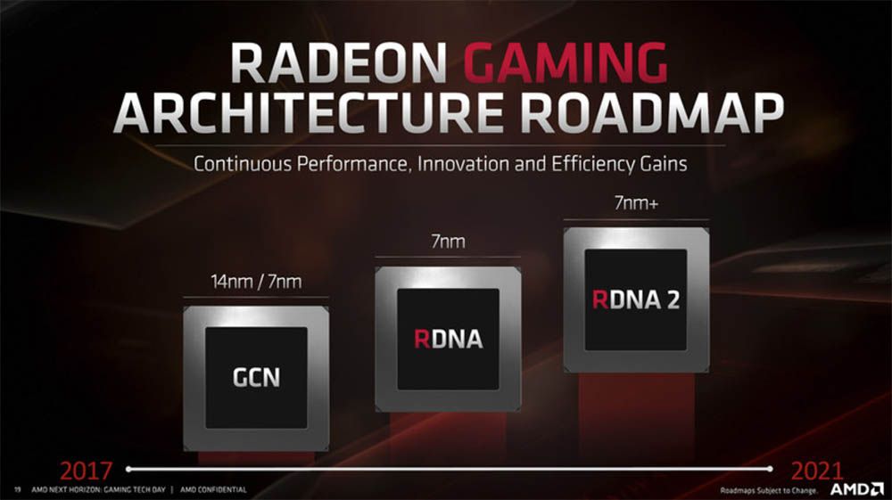
AMD is already producing Navi 21 at 7nm+ with the double size of Navi 10
Halfway through last year, AMD launched the Navi 10, at the heart of the Radeon RX 5700 XT, as the first sample of its new RDNA architecture, and even though not much time passed, theoptocrypto.com
It also makes sense regarding rumors that Sony originally planned for a 2019 launch. That original launch APU would've been Ariel, when they delayed it they upped the clocks from 1.8 GHz to 2 GHz and it turned into Oberon. That clock speed increase leads to loads of heat, which explains the devkit design.
https://www.overclock3d.net/news/systems/tsmc_is_rumoured_to_be_creating_a_new_7nm_console_chip/1 (April 2018)
https://www.neogaf.com/threads/poss...3-2ghz-clock-navi-10-based-gpu.1471267/page-3 (January 2019)
At least that makes a lot more sense than the alternative, that Sony designed one APU for a 2019 launch, then skipped it to create Ariel, then skipped that to create Oberon, did four more iterations of Oberon, while secretly working on the actual PS5 APU. That's a lot of money spent for creating designs you don't intend to use.
I've seen valid theories for the entire range. I just want it all to be over with, lol.
Last edited:
SmokSmog
Member
so you are saying the ps5 will have a 243w gpu, plus 50w for cpu and another 50 watts for ram, ssd and other stuff on the motherboard?
so a 350w console? just to save a few dollars on a bigger die with 20 more CUs?
No, just answered to this nonsense post from James Sawyer
Looks like Sony missed 2019 release date with Navi 10. Probably to TSMC low yield rate back in april.
I think Sony is going wide and fast
GitHub is true for BC only, but the clocks match the final console
54 CU @ 2.0 GHz
SlimySnake quick, how many TFlops is that?
Max 1,8GHZ for 36-40cus
Max 1700MHZ for +50cus
XSX 1700MHZ 56 CUs 12.2TF
PS5 unknown GPU 1700-1800MHZ
Last edited:
Roronoa Zoro
Gold Member
Yeah if they just have a general meeting where they at least go "capable of nearly 11 tf" or "capable of 4k gaming for next genYeah, I'm in the camp that it's not set in stone yet, when we take everything into account. I've went from 8tf-14tf, to 9tf-12tf. It's still wide open to me. We'll find out eventually, lol.
That's the thing, if. That's all we have right now is ifs. Again, github could be the final results. But I don't want the PS5 running at 2Ghz because they want to soften the PR hit, or get into TF tug of war with MS.
I've seen valid theories for the entire range. I just want it all to be over with, lol.
darkinstinct
...lacks reading comprehension.
There's now two products that were in the Github leak that turned out to be true (and at the exact same specs as in the test): Renoir and Arcturus. Plus takedown notices by AMD because of it. I'd say the "if" is getting smaller and smaller. Plus we have Cerny deflecting talk away from pure specs and towards SSDs. Do you do that with a powerful machine? And really Sony is not the odd one out here: We have heard for years that next gen we won't here a lot about teraflops and power, because due to Moore's Law slowing down and midgen refreshes the numbers won't look very impressive. And then we have Microsoft who made a monster (the One X) and then market their next gen console as "it eats monsters". I see two very different approaches here, one that is confident in their performance lead, another one that is talking about anything but performance (at least not GPU related performance). The strategies match the leak. And TBH Microsoft cannot afford to have a 9-10 TF machine for $500 follow a 6 TF machine for $500 three years earlier. That would be suicide. They have to do more and I wouldn't even be surprised if XSX is 600.
TeamGhobad
Banned
latest specs and sauce?
Captain Hero
The Spoiler Soldier
latest specs and sauce?
wait a minute I'm working on it
darkinstinct
...lacks reading comprehension.
latest specs and sauce?
Everybody is above 12.88 TF.
At least in Polaris equivalent TF.
SenjutsuSage
Banned
You displaying a classic case of using an extreme example to try prove your point. You painting a false picture by using Vega64 in your measurement of tflop efficiency. You should use a more common and widely accepted example and your point will be valid and fair.
It's an extreme example to you because Navi GPUs with the RDNA architecture are THAT much better per tflop than all other non Navi AMD GPUs. There is no more common and widely accepted example than the one I'm using because AMD hasn't had a GPU architecture this good in many years.
Find me one other AMD GPU since 2013 that with less teraflops can outperform another GPU from AMD's product lineup with notably more teraflops? GCN and its various revisions has been AMD's defacto architecture now for many years. These chips and their equivalent Nvidia parts in like for like teraflops are the things to compare to. AMD has commonly had a notable teraflop advantage over Nvidia cards, but where this never properly translated to performance, and now that we have AMD chips doing to those prior inferior AMD chips what Nvidia has been doing for years we are not suppose to use them as a point of comparison when it's precisely what's been happening with Nvidia versus AMD for years now?
I'm making the perfect comparison.
Captain Hero
The Spoiler Soldier
Insane Metal
Gold Member
That's perfect lol. You created it?
TeamGhobad
Banned
Everybody is above 12.88 TF.
At least in Polaris equivalent TF.
any sauce on this?
Captain Hero
The Spoiler Soldier
yes thats me sirThat's perfect lol. You created it?
Last edited:
- Status
- Not open for further replies.