The TSMC Technology Symposium is going on right now out in Santa Clara, and they've
unveiled a new technology, called Wafer on Wafer (WoW) which allows them to connect chips together without mounting them laterally on the same interposer, or using the likes of AMD's Infinity Fabric or Intel's EMIB designs to allow them to communicate.
The new wafer-stacking tech means chips can be piled on top of each other, much like the way NAND flash memory is being stacked in the latest solid state drives. The individual wafers are directly connected using through-silicon vias (TSVs) and will not only allow many more cores to be contained in a single package, but also allow them to communicate incredibly quickly too.
There is also the potential that these WoW designs can be jammed onto an interposer with other silicon to create proper monster chips. Or even have more than two wafers stacked on top of each other. Skyscraper GPUs, please!
There are inevitable drawbacks to this sort of manufacturing, and most of that is down to the wafer yields TSMC are getting from different technologies. With two wafers stacked on top of each other, if one of the chips comes out broken the connected chip is therefore useless, which would make wafer-stacking too costly on low-yield products.
That means it's more likely to be used on established production nodes with high manufacturing yields. That would cut down the wastage and still produce chips with far more power than their forebears. Again, this is how it works in SSD land too.
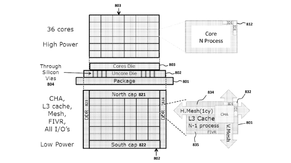
ntel have also filed
patents for stacked CPU technologies to allow them to combine older manufacturing processes with newer ones to create more advanced chips.
Given the high yield of something like TSMC's mature 16nm lithography it might not be beyond the realm of possibility for an old Pascal era chip to be 3D stacked, instantly doubling the core-count of the newborn GPU. Tasty. That would give multi-chip graphics cards a real boost, especially as they wouldn't actually need to appear as multi-GPU to the system.
Okay, right now that's a little far-fetched, and TSMC aren't going to divulge any further details about the new WoW tech until they're good and ready. But it does mean that TSMC, the biggest contract chip manufacturers in the world, will be able to offer their partners the capability to extend the lifetimes of their architectures on high-yield production nodes and deliver powerful silicon without struggling to stuff more cores into the same 2D space.
And that could be very exciting for future GPU refreshes. At the moment they're little more than rebadges – think RX 480 to RX 580 – but if AMD had the option to stack two Polaris 10 chips on top of each other that would have been a genuinely exciting refresh.


