What is found about Arden is that back-compat mode referrences Xbox One. Also number of CUs.Looks like some other people (M.Bluth on era) have found the same database and are starting to dig through. There are references to Arden = native, gen1, gen0. Just like Oberon. And the latest commits in those files are to Arden.
-
Hey Guest. Check out your NeoGAF Wrapped 2025 results here!
You are using an out of date browser. It may not display this or other websites correctly.
You should upgrade or use an alternative browser.
You should upgrade or use an alternative browser.
- Status
- Not open for further replies.
eastwood333
Banned
1. PS5 is more powerful than Xbox as stated by Klee and Jason.
2. The PS5 data is real and Xbox is more powerful, Klee and Jason have lost all credibility.
3. The PS5 data is real but Xbox is NOT 12 RDNA tflops, it is 12 GCN tflops that leaves Tom Warren, Microsoft, WC and Richard L. without credibility. And both consoles would be at the same power in this case.
They are going by there own trusted sources and are confident enough to say its a 12tf box. The evidence is beginning to pile up. DF,Tom Warren,Komachi,Dylan 522p,Windows Central,rogame,Arthur Gies,RedTechgaming now thinks XSX will be more powerful,and last,but not least,Phils own words and confidence in XSX being the most powerful next gen consoleIt's not confirmed by DF. They are assuming it is TF 12 Navi because Phil Spencer said GPU performance is 2x of X1X. Richard also said they asked MS is GPU in XSX 12 TF Navi, but didn't get any confirmation on that.
Last edited:
But that codename Sparkman jumps out. It doesn't fit with Arden (Shakespeare related). And Sparkman has way too high bw for it to be weaker Lockhart. How many CUs are in Sparkman? Or there's no info about it?What is found about Arden is that back-compat mode referrences Xbox One. Also number of CUs.
Last edited:
pawel86ck
Banned
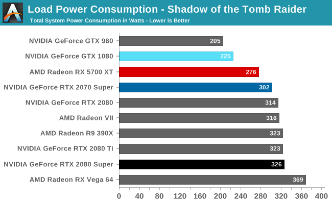
Here's chart made by DemonCleaner. As you can see 5700XT was pushed too high. 52CU with lower clock + RDNA2 architecture + 7nm+ would be way more power efficient.I'm basing it on the below Anandtech tests and Richard Leadbetter's expectation of XSX being >300W usage. He might be wrong but we'll see.
The 5700XT is alarmingly high (relatively) here. Even with efficiency gains and 7nm+ it would still be worrying.

Sparkman is Arden copy in this. It only shows max data because its theretical max for 14Gbps chip.But that codename Sparkman jumps out. It doesn't fit with Arden (Shakespeare related). And Sparkman has way too high bw for it to be weaker Lockhart.
Oberon has both VRS and RT.
Neander
Member
Few seconds later :

Carry on, Xbone fan! Thanks! Btw. at 6.30 Richard said the firm declined to comment on exact figure. So, later after your comment he said assume. So, he didn't confirmed it.
As opposed to you being a Sony fan? What's the point of this even?
It's pretty interesting to see people having mini meltdowns and denials at the prospect of a 12TF Xbox console though. Makes for great

")
Darius87
Member
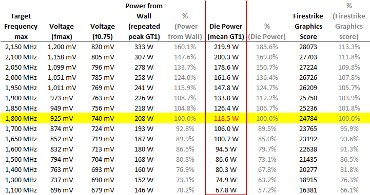
i did some reseach and good news is if we take into consideration PCM leak was
that's with 7nm litography with 7nm+(EUV) die size of 316nm2 could hold 56CU's with a bit real estate left, so 52CU at 2Ghz gets us 13+ Tflops for PS5.
PCB leak from May 21
May I remind you PCB leak is now 3/3.
256bit bus (Oberon AND Flute)
BW matching
Die size - 316mm² (pretty much 40CUs + Zen2 with some cache stripped)
PCB was leaked by guy who day after deleted his account but his avatar (piece od motherboard) and TOD of posting indicated someone from Asia. I always assumed these were "faster" dev kits Cerny mentioned and he wokred at TSMC.
that's with 7nm litography with 7nm+(EUV) die size of 316nm2 could hold 56CU's with a bit real estate left, so 52CU at 2Ghz gets us 13+ Tflops for PS5.
Last edited:
Nickolaidas
Banned
At this point all I want to see is live gameplay from both consoles to see what they're capable of. Those numbers fail to hype me anymore.
But...PS5 is 36CU 256bit part...?i did some reseach and good news is if we take into consideration PCM leak was
that's with 7nm litography with 7nm+(EUV) die size of 316nm2 could hold 56CU's with a bit real estate left, so 52CU at 2Ghz gets us 13+ Tflops for PS5.
Gamernyc78
Banned
Oh boy this thread is more bipolar than my x girlfriend 
CyberPanda
Banned
Aceofspades
Banned
I decided to wait for the reveals, chasing info in forums filled with attention seekers nerds got tiring for me.
Nickolaidas
Banned
He doesn't know anything about the Sony console
If he knew, he share it
Although, I also think that the console from microsoft will be stronger, but it will not affect almost anything, since Sony will again kill with their exclusives
Sorry if the truth offends someone \_( - +-)_/
Last edited:
LordOfChaos
Member
Copying my post over from the SSD thread because I like 'em

 www.neogaf.com
Sometimes I think people forget large sequential transfers aren't all there are to SSD performance.
Some points that may be interesting:
Pappa Cerny: . "The raw read speed is important," Cerny says, "but so are the details of the I/O [input-output] mechanisms and the software stack that we put on top of them. I got a PlayStation 4 Pro and then I put in a SSD that cost as much as the PlayStation 4 Pro—it might be one-third faster."
Again: "Rather than treating games like a big block of data [on PS5], we're allowing finer-grained access to the data"
Oftentimes it's not a big 20GB transfer that's going to be hitting an SSD, it's the unpredictable accesses to smaller files that really choke their performance, you're probably not hitting your drives max sequential rate most of the time.
What else gets rid of block level access and reaps big IOPS gains?
On Software Defined Storage:
"Our measurements show that SDF can deliver approximately 95% of the raw flash bandwidth and provide 99% of the flash capacity for user data. SDF increases I/O bandwidth by 300% and reduces per-GB hardware cost by 50% on average compared with the commodity SSD-based system used at Baidu," reads a 2014 study.
Thought for food
2)
The beauty of what I mentioned is no hardware change, a normal-ish PCI-e 4.0 drive plus software defined storage getting rid of block level accesses = massive IOPS.
Though I think the SSD will be more special than that with all their research and patents into controller SRAM caches and all that.
 www.freepatentsonline.com
- SRAM instead of DRAM inside the SSD for lower latency and higher throughput access between the flash memory controller and the address lookup data. The patent proposes using a coarser granularity of data access for data that is written once, and not re-written - e.g. game install data. This larger block size can allow for address lookup tables as small as 32KB, instead of 1GB. Data read by the memory controller can also be buffered in SRAM for ECC checks instead of DRAM (because of changes made further up the stack, described later). The patent also notes that by ditching DRAM, reduced complexity and cost may be possible, and cost will scale better with larger SSDs that would otherwise need e.g. 2GB of DRAM for 2TB of storage, and so on.
- The SSD's read unit is 'expanded and unified' for efficient read operations.
- A secondary CPU, a DMAC, and a hardware accelerator for decoding, tamper checking and decompression.
- The main CPU, the secondary CPU, the system memory controller and the IO bus are connected by a coherent bus. The patent notes that the secondary CPU can be different in instruction set etc. from the main CPU, as long as they use the same page size and are connected by a coherent bus.
- The hardware accelerator and the IO controller are connected to the IO bus.

If it ends up being all three parts of the triforce here...Holy hell.

SSD is the primary battleground of next-gen.
SSD prices aren't that bad these days. they have improved yeah but i just paid £380 for a 2TB SSD. this is an NVME one...ykno the one that will be in next gen consoles. not a slow SATA3 drive which is cheaper. there is no way they are sticking in a 1TB or 2TB SSD. also these drives run hotter...
Sometimes I think people forget large sequential transfers aren't all there are to SSD performance.
Some points that may be interesting:
Pappa Cerny: . "The raw read speed is important," Cerny says, "but so are the details of the I/O [input-output] mechanisms and the software stack that we put on top of them. I got a PlayStation 4 Pro and then I put in a SSD that cost as much as the PlayStation 4 Pro—it might be one-third faster."
Again: "Rather than treating games like a big block of data [on PS5], we're allowing finer-grained access to the data"
Oftentimes it's not a big 20GB transfer that's going to be hitting an SSD, it's the unpredictable accesses to smaller files that really choke their performance, you're probably not hitting your drives max sequential rate most of the time.
What else gets rid of block level access and reaps big IOPS gains?
On Software Defined Storage:
"Our measurements show that SDF can deliver approximately 95% of the raw flash bandwidth and provide 99% of the flash capacity for user data. SDF increases I/O bandwidth by 300% and reduces per-GB hardware cost by 50% on average compared with the commodity SSD-based system used at Baidu," reads a 2014 study.
Thought for food
2)
The beauty of what I mentioned is no hardware change, a normal-ish PCI-e 4.0 drive plus software defined storage getting rid of block level accesses = massive IOPS.
Though I think the SSD will be more special than that with all their research and patents into controller SRAM caches and all that.
INFORMATION PROCESSING DEVICE, ACCESS CONTROLLER, INFORMATION PROCESSING METHOD, AND COMPUTER PROGRAM - Sony Interactive Entertainment Inc.
<div p-id="p-0001">Disclosed herein is an information processing device including a host unit adapted to request data access by specifying a logical address of a secondary storage device, and a contro
www.freepatentsonline.com
- SRAM instead of DRAM inside the SSD for lower latency and higher throughput access between the flash memory controller and the address lookup data. The patent proposes using a coarser granularity of data access for data that is written once, and not re-written - e.g. game install data. This larger block size can allow for address lookup tables as small as 32KB, instead of 1GB. Data read by the memory controller can also be buffered in SRAM for ECC checks instead of DRAM (because of changes made further up the stack, described later). The patent also notes that by ditching DRAM, reduced complexity and cost may be possible, and cost will scale better with larger SSDs that would otherwise need e.g. 2GB of DRAM for 2TB of storage, and so on.
- The SSD's read unit is 'expanded and unified' for efficient read operations.
- A secondary CPU, a DMAC, and a hardware accelerator for decoding, tamper checking and decompression.
- The main CPU, the secondary CPU, the system memory controller and the IO bus are connected by a coherent bus. The patent notes that the secondary CPU can be different in instruction set etc. from the main CPU, as long as they use the same page size and are connected by a coherent bus.
- The hardware accelerator and the IO controller are connected to the IO bus.
If it ends up being all three parts of the triforce here...Holy hell.
If there really are such references then it would be nice if the one who found them could also post them somewhere.Sparkman is Arden copy in this. It only shows max data because its theretical max for 14Gbps chip.
Oberon has both VRS and RT.
But as I understand those Oberon tests are not even about RT or VRS. So even if there are no mentions of it, doesn't mean there's no RT or VRS capabilities.
Last edited:
D
Deleted member 471617
Unconfirmed Member
even if ps5 is 9.2 and x1 is 12 that's 30% difference in gpu power
Damn. That is a difference. I'm expecting PS5 to be no less than 10TF in GPU power which I guess would make Xbox 4 20% more powerful but even then, I have way more confidence in Sony's first party studios than I do Microsoft's to get every ounce of power out of the GPU and have some visual masterpieces.
With that said, I am hoping PS5 is 12TF and matches Xbox 4 because I want the best I can get for $500. Also, im NOT a fan of mid-gen consoles. I would prefer a 5 year generation and move on to PS6 instead of mid-gen console which will only introduce 8K resolution and thus, be the same as Pro/X - introduce something that maybe 5% of people have - a 4K (or in this case 8K) TV.
Just have to wait and see what happens.
Believe me, they are referrenced there, but not tested. Just have to look for it with a bit more care.If there really are such references then it would be nice if the one who found them could also post them somewhere.
But as I understand those Oberon tests are not even about RT or VRS. So even if there are no mentions of it, doesn't mean there's no RT or VRS capabilities.
it_wasn't_me
Banned
As opposed to you being a Sony fan? What's the point of this even?
It's pretty interesting to see people having mini meltdowns and denials at the prospect of a 12TF Xbox console though. Makes for great
Mini meltdowns and denials, yet you deliberately left out what Richard said few seconds later just to fits your narrative.
it_wasn't_me
Banned
i did some reseach and good news is if we take into consideration PCM leak was
that's with 7nm litography with 7nm+(EUV) die size of 316nm2 could hold 56CU's with a bit real estate left, so 52CU at 2Ghz gets us 13+ Tflops for PS5.
That's 10 TFLOPS RDNA which is around 0.9% stronger than XSX if XSX is 9.3 TF RDNA
BattleScar
Banned
It's possible, but it's highly unlikely. Pretty much impossible actually. Too much annoyance for developersHello !
A hardware with 2 APU is possible on a console like a GPU SLI on a PC ?
CyberPanda
Banned
it_wasn't_me
Banned
Sparkman is Arden copy in this. It only shows max data because its theretical max for 14Gbps chip.
Oberon has both VRS and RT.
Suddenly Oberon has both VRS and RT yet you, Xbone fans, claimed that PS5 in that case doesn't have yesterday because some OLD DATAMINE. Why flip-flop?
Last edited:
Psyrgery ES
Member
it_wasn't_me
Banned
Nobody has said it doesn't have except for some actual fanboys who have a horse in this race.Suddenly Oberon has both VRS and RT yet you, Xbone fans, claimed that PS5 in that case doesn't have. Why flip-flop?
Maybe you should relax a bit and stop throwing false claims and "Xbox fanboys" tag at everyone who implys PS5 might be weaker.
Be better off just separating the CPU off to get that die space and thermals for the GPU instead SLI. I think the Saturn might of had multiple GPUs but that was a mess to develop for. The arcade version of the dream cast naomi had a sli option with the elan board for triangle and lighting help to off load from CPU and was much better performance wise.Hello !
A hardware with 2 APU is possible on a console like a GPU SLI on a PC ?
Last edited:
it_wasn't_me
Banned
Nobody has said it doesn't have except for some actual fanboys who have a horse in this race.
Maybe you should relax a bit and stop throwing false claims and "Xbox fanboys" tag at everyone who implys PS5 might be weaker.
Nobody, but somebody said it.
 Btw. i've said numerous times Xbone fans. Cheers! Fans and fanboys isn't the same, though. I really don't like to call people fanboys even though they called me like that for reason.
Last edited:
wvnative
Member
What was it? Tweet is missing
What was this?
stopitgetsomehelp
Neo Member
Arcturus MI100
AMD 100-000000004-1
SCLK ~930 ( SOCCLK? )
MCLK ~1740 (suspiciously closer to 14Gbps GDDR6)
FCLK ~1200 (no idea)
HeisenbergFX4
Gold Member
The deleted Tweet read:
Arcturus MI100
AMD 100-000000004-1
SCLK ~930 ( SOCCLK? )
MCLK ~1740 (suspiciously closer to 14Gbps GDDR6)
FCLK ~1200 (no idea)
From Rogame
Arcturus MI100
AMD 100-000000004-1
SCLK ~930 ( SOCCLK? )
MCLK ~1740 (suspiciously closer to 14Gbps GDDR6)
FCLK ~1200 (no idea)
From Rogame
So direct your anger to the ones who said it. You just called r600 an Xbox fanboy about a claim he hasn't even made?Nobody, but somebody said it.
Last edited:
it_wasn't_me
Banned
So direct those claims to the ones who said it. You just called r600 a Xbox fanboy about a claim he hasn't even made.
I've said Xbone fans! Don't twist it, Xbone fan!
CyberPanda
Banned
A tweet from Ro and Komachi.Twits are no longer avaiable.
What was in them?


CyberPanda
Banned
Arcturus is for compute, and is possibly going to be used for workstations. I'm guessing Azure.Arcturus has 128CUs lol
joe_zazen
Member
This is just plain wrong. As a public company having stock in the NYSE (New York Stock Exchange), the SEC requires that all public companies (MSFT) divulge their financial data to the public.
I think your phrasing was incorrect.
MS does not divulge specific numbers wrt gaming division. They get lumped, or has that changed?
CyberPanda
Banned
Norse
Member
I think you could use a time out.I've said Xbone fans! Don't twist it, Xbone fan!
it_wasn't_me
Banned
CEO of AMD saying RDNA TF > GCN TF in Navi conference.
Some random tweet: TF is TF.
For the purpose of marketing i presume.
Psyrgery ES
Member
He was asked if he believed the Xsx would be the most powerful console and he replied "Yes".
Fake
Member
The real question is: Who to believe?For the purpose of marketing i presume.
it_wasn't_me
Banned
I think you could use a time out.
Then this can be applied to others which are more extreme than me.
Last edited:
CyberPanda
Banned
YepHe was asked if he believed the Xsx would be the most powerful console and he replied "Yes".
stopitgetsomehelp
Neo Member
CEO of AMD saying RDNA TF > GCN TF in Navi conference.
Some random tweet: TF is TF.
TF is just a number based on GPU specs.
On the other hand we have performance on different architecture. RDNA > GNC, obviously.
HeisenbergFX4
Gold Member
If PS5 launches at $399, I dont think it will matter which system is more powerful. PS5 would sell like hotcakes at $399.
Its all about price.
Anyone can build a monster but make it affordable for the masses?
Look forward to full reveals including pricing.
- Status
- Not open for further replies.