• Hey, guest user. Hope you're enjoying NeoGAF! Have you considered registering for an account? Come join us and add your take to the daily discourse.

Next-Gen PS5 & XSX |OT| Console tEch threaD

Status
Not open for further replies.

TeamGhobad

Banned
The big advantage is you can shrink your vanilla 7nm design to 6nm with little retooling/investment
So say Sony uses a 400mm2 SoC on late 2020 they can shrink to 340mm2 in 2021 for cost reductions

why not just directly go 6nm?
 
Last edited:

stetiger

Member
Jason from kekaku

lol no, the strength of the 7nm process is in the density increase not the performance/clocks
Consoles will go with 64 to 72CUs total (56 to 64 enabled respectively)

My prediction is 11TF minimum for a $399 system
12-13TF for $499

7nm doesn't have as much performance increment as past node transitions, its strenght is in the density increase

Which is why i think anything less than 56CUs (enabled) is not happening.

64CUs (72 total - 8 disabled) at 1500 Mhz = 12.2TF on plain 7nm is doable
If they go with 7nm EUV 13-14TF is possible

Who set the bar there though?
Sony/MS are not aiming for some artificial ceiling, they will aim to create the fastest boxes technology allows for $500, every bit of performance counts for a proper next gen leap, 4k alone will eat a huge chunk of resources.

Not to mention that 36CU chip is clocked way to high fit on a console. They'll need to downclock it for console and then its below Vega64 territory.
The best bet is a 64 to 72 CU chip

Not likely, 64 CUS would be too big unless they forgo the IO bridge, redesign L3 Cache and ship a monolithic chip. If they can do that, then yeah but that seems unlikely. It's time to accept 10TFLOPS, if anything 10.8 to have marketing edge on stadia.

so these consoles can and most likely will be 6nm. interesting. i think 12tflops is back on the menu boys.
Noticed how Stadia is using Vega? It's because the chip needs to be designed and manufactured 1year in advance. Don't expect 6nm on consoles. Next year, but maybe in 2021 which would allow them to sell at a small loss at launch and recuperate that loss the following year.
 
Ehmmm.... there will be not that many CUs!?

Are you a 8TF flat earther? ;)

Both systems will be at least 12.0 teraflops.

I'd be surprised if either has less than 56 active CUs.

Likely scenario:
  • Sony: 56 active @ 1800
  • MS: 60 active @ <1800
These are consoles that are supposed to last a generation (7-8 years) from release (2020).

Navi is a semi custom customer driven part. Neither Sony or MS will want to leave any perf on the table.
 

SonGoku

Member
Not likely, 64 CUS would be too big unless they forgo the IO bridge, redesign L3 Cache and ship a monolithic chip. If they can do that, then yeah but that seems unlikely. It's time to accept 10TFLOPS, if anything 10.8 to have marketing edge on stadia.
Here is my estimate
72CU APU = 399.1 mm2
64CU APU = 385.6 mm2

Bolded imo is the perf/buck sweetspot

For reference
The RTX 2060 is 445mm2 $349 with Nvidia's high profits
Launch PS4 roughly 350 mm2 at $399

56CUs at 1500-1600Mhz = 10.7-11.4TF
64CUs at 1500-1600Mhz = 12.2-13.1TF
7nm EUV in for end of 2020 could happen.
Yep :)
 
Last edited:
It's funny to see everyone (including myself) now lowering their TF expectations.

Digital Foundry actually said not to expect more than about 10..!
 

TeamGhobad

Banned
Here is my estimate
72CU APU = 399.1 mm2
64CU APU = 385.6 mm2

Bolded imo is the perf/buck sweetspot

For reference
The RTX 2060 is 445mm2 $349 with Nvidia's high profits
Launch PS4 roughly 350 mm2 at $399

56CUs at 1500-1600Mhz = 10.7-11.4TF
64CUs at 1500-1600Mhz = 12.2-13.1TF

Yep :)

the added cost of SSD and RT and these consoles will surely be 599.
 

MadAnon

Member
I edited my post:


56CUs at 1500-1600Mhz = 10.7-11.4TF
64CUs at 1500-1600Mhz = 12.2-13.1TF

You can bookmark my post consoles won't be smaller than 56CUs enabled

The big advantage is you can shrink your vanilla 7nm design to 6nm with little retooling/investment
So say Sony uses a 400mm2 SoC on late 2020 they can shrink to 340mm2 in 2021 for cost reductions

64CU APU = 385 mm2

flat,550x550,075,f.u1.jpg


Navi is 251 mm2 if you missed it. 64CU would be 400 mm2. Now add CPU cores and you have a 500mm2 APU.

giphy.gif
 
Last edited:

SonGoku

Member
Firstly, I don't think PS5 is using chiplet(s).
Yeah I don't think so either
I was just confused about the separate Zen2 IO die but we cleared it up a few pages back
Likely scenario:
  • Sony: 56 active @ 1800
  • MS: 60 active @ <1800
With RDNA new CU config you have to disable 8 CUs at a time
Btw how do you propose they reach 1.8Ghz while staying under 200W? 7nm EUV?

(72CUs total - 8 disabled) 64CUs at 1580MHz gives the prized 12.9TF
Reports say Navi is 251 mm2 if you missed it. 64CU would be 400 mm2. Now add CPU and you have some 500mm2 APU
Thats not how it works my friend, CUs take less than 50% of die space. Its not a linear increase
Calculations were posted here #4,276
5700:
GDDR6 phy controller: 4.5mm x 8
Dual CU: 3.37mm x 20
4 ROP cluster: .55mm x 16
L1+L2+ACE+Gemotry processor+empty buffer spaces + etc: 139mm

378.8mm2

75mm for CPU
45mm for 10 GDDR6 controllers
8.8mm for ROPs
140mm for buses, caches, ACE, geometry processors, shape etc. I might be over estimating this part as the 5700 seems to have lots of "empty" areas.

We have ~110mm left for CUs + RT hardware. There is enough there for ~30 dual CUs and RT extensions.
 
Last edited:

LordOfChaos

Member
N7 Pro is also going into mass production soon for the September iPhone, that's a much higher volume product than a console and Apple is absolutely not stingy on die area/transistor budget. It's based on 7nm+, and might be exclusive, but that should say something about N7+ yields.

A12 @ 6.9(nice) billion transistors, A12X at over 10 billion


Now awaiting TSMC N7+ Pro, N6 Pro, N7DoublePlusGoodPro...
 
Last edited:
Yeah I don't think so either
I was just confused about the separate Zen2 IO die but we cleared it up a few pages back

With RDNA new CU config you have to disable 8 CUs at a time
Btw how do you propose they reach 1.8Ghz while staying under 200W? 7nm EUV?

(72CUs total - 8 disabled) 64CUs at 1580MHz gives the prized 12.9TF

Assuming we have 64 CUs on the die. 8 Shader engines with 8 CUs per shader engine. Disabling 1 CU in each shader engine gets you to 56 CUs active.

Edit: I don't think Sony will have more than 64 CUs on the die in total. When Sony took their "branch" of the master Navi project to work from, it still likely had the 64 limit. Just a guess. Just how MS will have taken a snapshot of the current Navi implementation when they started. Each party working on their own, not knowing what the other is up to. For projects in development for a long time they could have drastically changed from the original foundation of the project. Which is why neither party is absolutely sure what the other has at this current point in time.

Undervolt, overclocking and possibly 7nm+ to get the power requirements down.

I think PS5 has been put together with the power hungry GPU in mind. How could it not be? It's one of the most important things in a console. Also, it's AMD, people must have known what they were up against going in. So how do you reduce the power budget? Get rid of RAM. But if there's less RAM (16gb usable) we need a faster data on demand from storage. So, we drop the hard disk and replace with SSD, which is also less power hungry. SSD still isn't fast enough so we need to turbo charge it somehow. We need to trim the power budget more, so we go with HBM/DDR4 as it's less power hungry than vanilla GDDR6. We're still over budget, so we wait for the next node shrink... etc
 
Last edited:

SonGoku

Member
N7 Pro is also going into mass production soon for the September iPhone, that's a much higher volume product than a console and Apple is absolutely not stingy on die area/transistor budget. It's based on 7nm+, and might be exclusive, but that should say something about N7+ yields. A12 @ 6.9(nice) billion transistors, A12X at over 10 billion
Now awaiting TSMC N7+ Pro, N6 Pro, N7DoublePlusGoodPro...
Also relevant
TSMC’s CEO said the company has started volume production of its 7N+ process technology, DigitTimes reported on Friday. It is the company’s first process node to use EUV on a few critical layers. The company says the yield is on par with 7nm.
 
Last edited:

SonGoku

Member
So how do you reduce the power budget? Get rid of RAM. But if there's less RAM (16gb usable) we need a faster data on demand from storage. So, we drop the hard disk and replace with SSD, which is also less power hungry. SSD still isn't fast enough so we need to turbo charge it somehow. We need to trim the power budget more, so we go with HBM/DDR4 as it's less power hungry than vanilla GDDR6. We're still over budget, so we wait for the next node shrink... etc
Yeah i hope they dont compromise on ram, it should match the XB2 24GDDR6
Im just curious why you stuck with that 1.8GHz number, RDNA2 will likely break the 64CU limit so you can reach better perf/watt with a bigger chip clocked lower
 
Last edited:
Yeah i hope they dont compromise on ram, it should match the XB2 24GDDR6
Im just curious why you stuck with that 1.8GHz number, RDNA2 will likely break the 64CU limit so you can reach better perf/watt with a bigger chip clocked lower

I don't think RDNA2 would fit the timescales for either Sony or MS. They may lift some features from it and drop them into their ongoing implementation based on much earlier Navi snapshots when they each began their projects. So I think both will be living with a 64 CU limit.

For me the reddit dev summit leak has been the most credible so far (56@1800=12.9). As I've been to events like that in the past. Which is strangely, what gives the glimmer of hope for #team14.2 which I'll expand on later.
 

SonGoku

Member
7nm+ it is then
Let's not declare victory just yet, yields on mobile chips are on par. Here is hoping it will be ready for big chips come mid 2020. I think its likely
I don't think RDNA2 would fit the timescales for either Sony or MS
AMD has a history of putting new tech on consoles, its also in their best interests both consoles are RDNA2 to guarantee a generation of games optimized for their current GPU arch
For me the reddit dev summit leak has been the most credible so far (56@1800=12.9). As I've been to events like that in the past. Which is strangely, what gives the glimmer of hope for #team14.2 which I'll expand on later.
That might have been a placeholder, the only reasonable way to reach 14TF+ on consoles i can think off is through 7nm EUV on a 72CU chip (64 enabled) at 1750MHz
 
Last edited:
the added cost of SSD and RT and these consoles will surely be 599.
There are rumors that the PS5 might actually cost $599 (BoM), but Sony is willing to offer it for $499 thanks to their PSN revenue.

N7 Pro is also going into mass production soon for the September iPhone, that's a much higher volume product than a console and Apple is absolutely not stingy on die area/transistor budget. It's based on 7nm+, and might be exclusive, but that should say something about N7+ yields.

A12 @ 6.9(nice) billion transistors, A12X at over 10 billion


Now awaiting TSMC N7+ Pro, N6 Pro, N7DoublePlusGoodPro...
Mobile SoCs have small die sizes (~100mm2), so:

Wafer_die%27s_yield_model_%2810-20-40mm%29_-_Version_2_-_EN.png
 

LordOfChaos

Member
There are rumors that the PS5 might actually cost $599 (BoM), but Sony is willing to offer it for $499 thanks to their PSN revenue.


Mobile SoCs have small die sizes (~100mm2), so:

Wafer_die%27s_yield_model_%2810-20-40mm%29_-_Version_2_-_EN.png


PS4 lifetime sales are just over 90 million, Apple sells some 40 million iPhones a quarter, even at smaller die sizes that needs a lot of viable silicon. And that's launching almost a year before the 9th gen consoles.
 
Last edited:
PS4 lifetime sales are just over 90 million, Apple sells some 40 million iPhones a quarter, even at smaller die sizes that needs a lot of viable silicon. And that's launching almost a year before the 9th gen consoles.
Yeah, they use a lot of wafers, but the chance of defects is much lower, so they have less wasted dies. There's a reason Apple used 7nm chips before than anyone else (PC GPUs, consoles).

This probably explains why Navi cards are not so cheap compared to Zen 2 CPUs. Yields aren't that good (yet).
 
Keep in mind though 7nm EUV isn't a new process node, so transition from 7nm to 7nmEUV wont be harsh
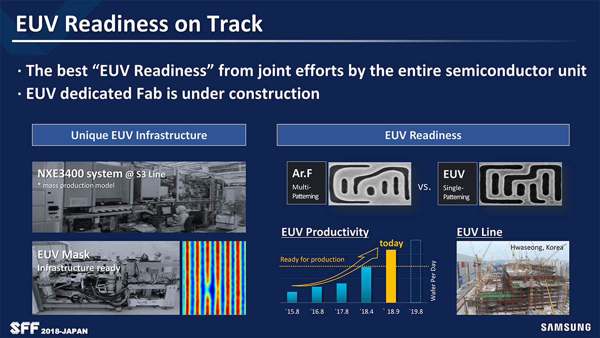
Not sure if Navi/Zen 2 use EUV, but it definitely seems to help (notice the etching pattern):

8.png


Maybe this will allow next-gen consoles to hit the 12 TF target next year?
 

ethomaz

Banned
What that means?


What rumors?

Edit -Now I understood... seems like some rumors about Anaconda was controlled leaks... these from "Insiders".
 
Last edited:
  • Like
Reactions: TLZ

SonGoku

Member
Not sure if Navi/Zen 2 use EUV, but it definitely seems to help (notice the etching pattern):
RDNA2 "nextgen" will be on 7nm EUV (What i predict next gen consoles will use) since consoles APU its semi custom they can port ZEN2 to 7nm EUV or RDNA2 to 7nm
Another possibility is big ass APU chip on 2020 and shrink to 6nm on 2021.
Maybe this will allow next-gen consoles to hit the 12 TF target next year?
If 7nm EUV is available at launch 13-14TF will be a reality
 
Last edited:

ethomaz

Banned
TFlops Navi/RDNA =/= TFlops Vega/GCN
Well actually they are the same :D

Just the efficiency (use) in gaming is different and Navi is nowhere close to nVidia yet (7.5TFs nVidia card fighting against 10TFs Navi card).
 
Last edited:

Ellery

Member
Even though I see it the other way feeling it is virtually impossible to get 12TF or higher and think he is dead wrong I can still admire the faith and dreams SonGoku has for the next generation.
 

joe_zazen

Member
, if sony did something similar it would be good for gamers right?

I think it comes down to philosophy and taste, so my answer is no.

In my judgement, the worst games are free games or games with a very low price, where developers cannot rely on entrance fee to make a living. So anything that disrupts the “we make our money from the purchase price of our game”, I see as a negative. Right now, console gaming is still driven by premium gamers willing to buy games upfront. YAY! That may change if f2p and $5 buffet gamers become the majority. BOO!

Now, some people prefer games like Fortnite or candy crush or Las Vegas Slots Royale; just like some people prefer free to air commercial tv over things like hbo. I am sure they will disagree and would be happy with a free to play or $5 per month all you can buffet.
 

ethomaz

Banned
Could this disparity be explained by tiled rendering (which Navi doesn't seem to have)?
It is one of the reasons for sure but here are a lot of things nVidia does that AMD not.
AMD always did better in compute tasks with GCN and that was his big selling point in the Prosumer market.
RDNA now dropped the Prosumer to focus only in games... GCN continue being for Pro/HPC market.
 
Last edited:

SonGoku

Member
Could this disparity be explained by tiled rendering (which Navi doesn't seem to have)?
Navi is already close to Pascal which has it
Must be further Turing improvements
DemonCleaner DemonCleaner post: #1,276
turing is more flop efficient compared to pascal because they use concurrent integer processing which isn't taken into acount in the FLOP number. it comes at a rather big price for die area real estate. one has to keep that in mind.
 
Last edited:

yurinka

Member
You'll see :)
For the record
11TF at $399
12-13TF at $499
I think Sony will go with between 11 and 12TF at $499.

I think DS5 will have some of the patented VR related stuff: splittable, extra cameras or sensors for better tracking and allow finger tracking, maybe touchscreen instead of touchpad and lightbar... so these pads will be expensive and I think they'll use them both as standard DualShock and to avoid people having to get additional controllers for VR with the idea of lowering the PSVR2 entry price.

Scarlett would get the same 11-12TF at $399 but with no fancy controller bundled and some Game Pass months instead.
 
Last edited:

SonGoku

Member
N Negotiator

Figure 5 shows that the mix of integer pipe versus floating point instructions varies, but across several modern applications, we typically see about 36 additional integer pipe instructions for every 100 floating point instructions. Moving these instructions to a separate pipe translates to an effective 36% additional throughput possible for floating point.
A third factor to consider for Turing is the introduction of integer execution units that can execute in parallel with the FP32 CUDA cores. Analyzing a breadth of shaders from current games, we found that for every 100 FP32 pipeline instructions there are about 35 additional instructions that run on the integer pipeline. In a single-pipeline architecture, these are instructions that would have had to run serially and take cycles on the CUDA cores, but in the Turing architecture they can now run concurrently. In the timeline above, the integer pipeline is assumed to be active for about 35% of the shading time.
More here
Turing is a work of art really
 
Last edited:
I've seen that before, but I'm not sure where INT32 shaders are useful in modern video games. I thought they had moved to FP32 long time ago (GeForce 256 for T&L and GeForce 8 for both pixel/vertex shaders).

Still, I think Navi would greatly benefit by licensing PowerVR's TBDR, along with HW RT.

How are they going to pitch Navi (without tiled rasterization) against competing mobile GPUs?
 
That might have been a placeholder, the only reasonable way to reach 14TF+ on consoles i can think off is through 7nm EUV on a 72CU chip (64 enabled) at 1750MHz

Not necessarily...

  • 56 @ 1800 = 12.9
  • 60 @ 1850 = 14.2
Having the redundancy of 4 disabled CUs across 64 CUs might just let you push the yield enough to make it viable from a cost perspective.

I said that the dev summit leak of 12.9 was the only thing giving hope to #team14.2TF. Why? Read on...

Both Sony and MS have been tight as a drum with leaks this generation. Likely because everyone involved is NDA'd up to the eyeballs and the risk of violating it just isn't worth losing your job and more for.

In the Wired interview, Cerny said the reason to get this information out there was that kits etc were going out to developers shortly and they wanted to pre-empt the release of information.

So then what happens? A reddit post goes up with the specs gleamed from the dev summit. Coincidence? Then to add fuel to the fire a picture from the summit is posted where Sony logos can be seen around the venue. Who takes random ass photos at a dev summit?

So either it's a dev leaking the actual values, possible but unlikely due to strict NDAs (where are all the other leaks?) or it's Sony deliberately muddying the waters with their own leak. If you're going to leak your own info, it needs to be your own advantage. To feed the fanboys? Unlikely. To make MS think they've got the goods and a real performance target to aim at? Oh yes, now that's where it gets interesting...

  • Fake leak 12.9
  • MS work towards beating the supposed PS5 12.9 perf target
  • Sony slow drip information to collaborate 12.9
  • MS trumpets their 13.5 tf masterpiece expecting they've hit a home run
  • Sony comes in and does a mic drop of 14.2
So if you're in MS position, do you take the chance and crow about your achievement of beating 12.9? Knowing that it could blow up in your face.

I think they're slowly figuring out that every leak has been fabrication to lead them down the garden path.

From a customer perspective I think this is amazing because it practically guarantees 12.9 as a minimum.
 
Last edited:

SonGoku

Member
I've seen that before, but I'm not sure where INT32 shaders are useful in modern video games. I thought they had moved to FP32 long time ago (GeForce 256 for T&L and GeForce 8 for both pixel/vertex shaders).

Still, I think Navi would greatly benefit by licensing PowerVR's TBDR, along with HW RT.

How are they going to pitch Navi (without tiled rasterization) against competing mobile GPUs?
A third factor to consider for Turing is the introduction of integer execution units that can execute in parallel with the FP32 CUDA cores. Analyzing a breadth of shaders from current games, we found that for every 100 FP32 pipeline instructions there are about 35 additional instructions that run on the integer pipeline. In a single-pipeline architecture, these are instructions that would have had to run serially and take cycles on the CUDA cores, but in the Turing architecture they can now run concurrently. In the timeline above, the integer pipeline is assumed to be active for about 35% of the shading time.
Seems to explain how Turing punches above its weight compare to Pascal
Still, I think Navi would greatly benefit by licensing PowerVR's TBDR, along with HW RT.
No doubt that would be a dream
How are they going to pitch Navi (without tiled rasterization) against competing mobile GPUs?
I think Navi already has some form of tiled rasterization, weren't there patents
Having the redundancy of 4 disabled CUs across 64 CUs might just let you push the yield enough to make it viable from a cost perspective.
You can't disable in groups of 4CUs anymore in RDNA
From a customer perspective I think this is amazing because it practically guarantees 12.9 as a minimum.
I don't disagree with what you are getting at its the execution where i think different.
btw what total power consumption are you speculating for PS5?
 
Last edited:
You can't disable in groups of 4CUs anymore in RDNA

I don't disagree with what you are getting at its the execution where i think different.

I'm not sure whether I've misunderstood you or I've not explained my earlier posts clearly enough.

The idea wasn't to disable a single group of 4 CUs out of the total 64 CUs on the die.

But to disable 4 in total - the faulty ones. Each of which could be anywhere in the die. Ideally evenly spreading the disabled CUs over the available shader engines.

Disabling only each faulty CU would be preferred. But RDNA slides show dual compute units. It may mean that you can only disable the dual CU unit rather than individually. So for each faulty CU, you'll likely be taking it's conjoined healthly twin one out of action too? This is assuming that the semi-custom layouts used for PS5 and Anaconda are very similar to the released RDNA info which may not be the case.
 
Status
Not open for further replies.
Top Bottom