-
Hey Guest. Check out your NeoGAF Wrapped 2025 results here!
You are using an out of date browser. It may not display this or other websites correctly.
You should upgrade or use an alternative browser.
You should upgrade or use an alternative browser.
- Status
- Not open for further replies.
FranXico
Member
If this Microsoft two console rumor is true what if the weak one is similar power to the PS5 and the second one is beast around $600, would you still buy it?
i presume you just dont know what your talking about.. rather than deliberately spreading miss-information.
Night.Ninja
Banned
Lort articulates my thoughts on this post better than I possibly could:
This whole thread is 70% speculation no?
FranXico
Member
Sure it is. Based on what exactly, are you assuming that the PS5 will be closer in power to the weaker Xbox than to the stronger one?This whole thread is 70% speculation no?
Night.Ninja
Banned
Sure it is. Based on what exactly, are you assuming that the PS5 will be closer in power to the weaker Xbox than to the stronger one?
it was a question, you warriors see weak and ps5 and get emotional
bitbydeath
Gold Member
If this Microsoft two console rumor is true what if the weak one is similar power to the PS5 and the second one is beast around $600, would you still buy it?
You wouldn't get much more power with only throwing in an additional $100.
TLZ
Banned
It wouldn't be worth it imo.If this Microsoft two console rumor is true what if the weak one is similar power to the PS5 and the second one is beast around $600, would you still buy it?
Fake
Member
Next-Gen PS5 & XSX |OT| Console tEch threaD
That's because of the PS5 Wired soft reveal, Xbox dint have anything of the sort yet If you do find a leak/rumor that is worth discussing let me know to add to the OP Exactly.
FranXico
Member
Ok, first, to answer your question: No. I probably wouldn't buy any of the three consoles, to be honest. Especially without any kind of ballpark for specs.it was a question, you warriors see weak and ps5 and get emotional
Gamernyc78
Banned
They'd tell you they're "socializing"
When all they do is either post about themselves or find something to rage about, both revolve around attention seeking.
I don't know about your surroundings and culture, but believe me it's still looked at that way in many places. I still hide (cover) mine when guests come over. I don't want that stigma hovering over me. People love talking shit. It's not right, but I'd rather stay away from all that and keep it to myself than having to deal with shitty looks and backbiting.
Heh. Almost similar story re NES. I got my Famicom in '90, when SNES was released. Like, imagine buying a PS4 next year, right after the PS5 is released. And all I had to play with until '90 was my Atari 2600. Ugh.
I was lucky my friend had a SNES that I played a lot, which he also lent me a good number of times, which was very cool of him.
")
I'm in NYC and almost every home I go to has a console as it's Centerpiece media hub. My living room has literally a shrine to gaming, bought a projector just for my ps4 and when I throw parties my ps4 goes right on to YouTube and thts how I play music. The last time I think anybody viewed gaming as kiddy in my immediate circle was when I was 11, mind you I'm 40 now. I'm not saying around your circle is not viewed that way but definitely not around mine. Plus like I said adult sports stars, rappers, actors alike talk about gaming more often than I remember before.
SonGoku
Member
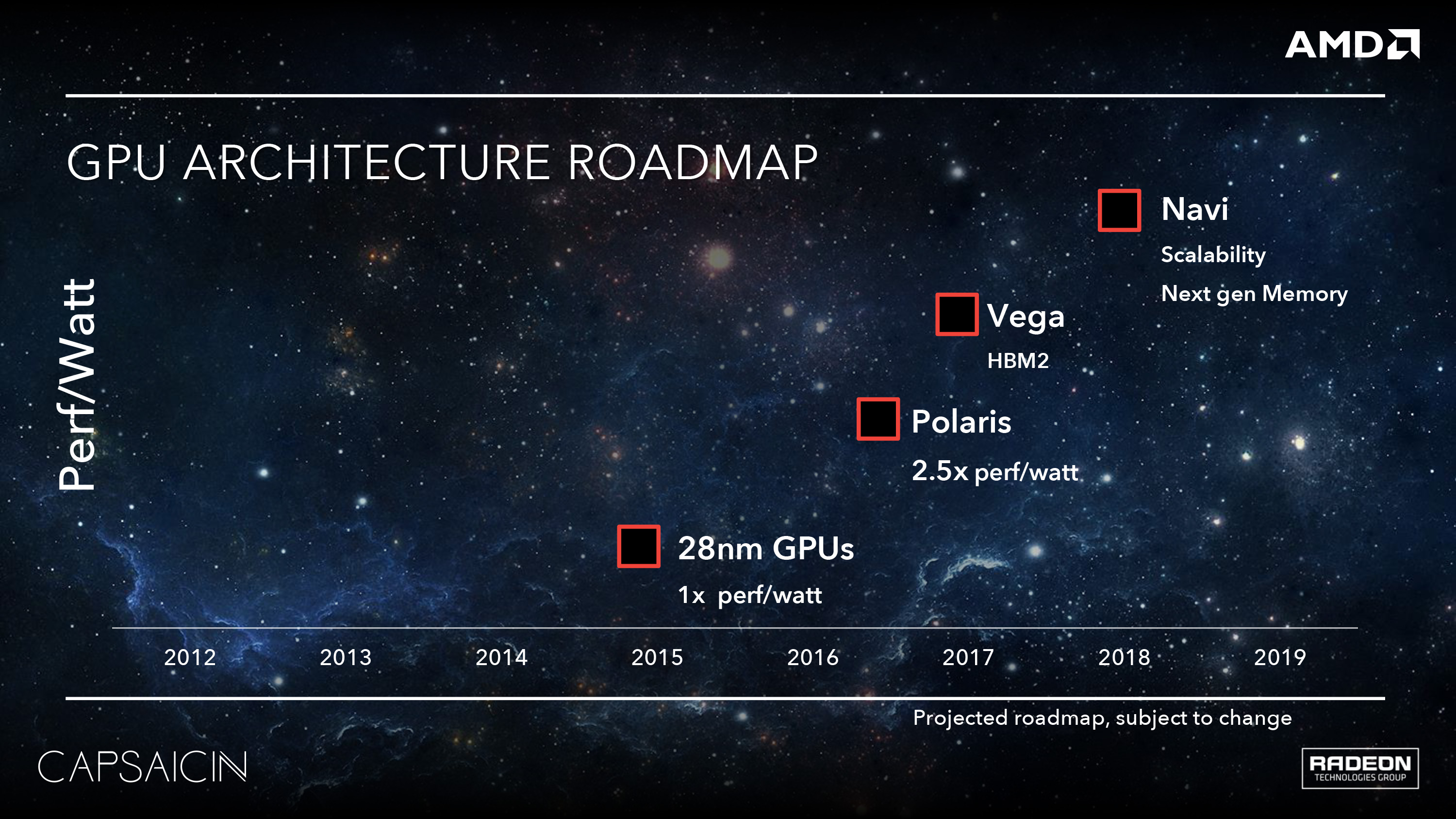
Im not saying 13TF will happen (currently siding towards 12TF) but you are being disingenuous with your comparison.For you to have a 13TF console, you'd need roughly ANOTHER 50%+ improvement compared to the 225w Navi that was just announced.
Highly doubt it.
RX 5700 cards are 48CUs at most and pushing clocks well beyond diminishing returns (hence the increased power consumption). Just how Polaris had worse perf/watt than vega
RX5700 series are also first gen Navi on the new 7nm process so yields aren't the best and the possibility of it being hybrid gcn-rdna further skews comparisons
TLZ
Banned
You're a lucky man. Wish I had that.I'm in NYC and almost every home I go to has a console as it's Centerpiece media hub. My living room has literally a shrine to gaming, bought a projector just for my ps4 and when I throw parties my ps4 goes right on to YouTube and thts how I play music. The last time I think anybody viewed gaming as kiddy in my immediate circle was when I was 11, mind you I'm 40 now. I'm not saying around your circle is not viewed that way but definitely not around mine. Plus like I said adult sports stars, rappers, actors alike talk about gaming more often than I remember before.
Imtjnotu
Member
So where did your bullshit rumor of the PS5 being close to Lockhart come fromOh so rumors are facts now, I never knew

Night.Ninja
Banned
So where did your bullshit rumor of the PS5 being close to Lockhart come from
Sony aint cutting you a cheque, you are getting to emotional

Insane Metal
Gold Member
"You" warriors huhit was a question, you warriors see weak and ps5 and get emotional
Negotiator
Banned
Lockhart will be a $299, 1080p focused console (~5TF). PS5 targets 12-13TF and there's no way it's gonna cost less than $499.
Unless they're willing to do heavy subsidizing (don't expect more than $100)...
Unless they're willing to do heavy subsidizing (don't expect more than $100)...
Sony aint cutting you a cheque, you are getting to emotional
That is twice in as many posts you are pulling the fanboy card to a rather benign question.
If you are not here to discuss the reasons behind your speculations, and rather project with 'fanboy' responses when questioned, then don't post in here.
Night.Ninja
Banned
Yes warriors you people who get overly emotional about consoles"You" warriors huh
Imtjnotu
Member
Sony aint cutting you a cheque, you are getting to emotional
Emotional
have you seen my posting historyNight.Ninja
Banned
That is twice in as many posts you are pulling the fanboy card to a rather benign question.
If you are not here to discuss the reasons behind your speculations, and rather project with 'fanboy' responses when questioned, then don't post in here.
It's fucking speculation like most majority of posts in here I didn't claim to be a insider.
I'm just throwing out a thought and people are getting emotional
DeepEnigma
Gold Member
It's fucking speculation like most majority of posts in here I didn't claim to be a insider.
I'm just throwing out a thought and people are getting emotional
You never responded to my question when you asked, just focused on the "fanboy" side of things.
It's fucking speculation like most majority of posts in here I didn't claim to be a insider.
I'm just throwing out a thought and people are getting emotional
You are the one who is overreacting and getting hostile in the discussion.
People were asking you to clarify and you projected your rhetoric. Have a little time out, and relax.
TeamGhobad
Banned

joe_zazen
Member
I'm in NYC and almost every home I go to has a console as it's Centerpiece media hub. My living room has literally a shrine to gaming, bought a projector just for my ps4 and when I throw parties my ps4 goes right on to YouTube and thts how I play music. The last time I think anybody viewed gaming as kiddy in my immediate circle was when I was 11, mind you I'm 40 now. I'm not saying around your circle is not viewed that way but definitely not around mine. Plus like I said adult sports stars, rappers, actors alike talk about gaming more often than I remember before.
Depends on how successful a person is on how the things they are interested in get judged. Have an apartment overlooking central park? stuff it full of anime figurines and gaming memorabilia, people wont say shit. Still live at home with parents in late 30s? Yeah people will judge your gaming habit, you bet.
CrustyBritches
Gold Member
Polaris had better perf/watt than Vega when using valid RX 470 vs Vega 56 and RX 480 vs Vega 64.Im not saying 13TF will happen (currently siding towards 12TF) but you are being disingenuous with your comparison.
RX 5700 cards are 48CUs at most and pushing clocks well beyond diminishing returns (hence the increased power consumption). Just how Polaris had worse perf/watt than vega
The chip that came the following year, RX 580 had much worse perf/watt...
Firstly, that's why I say to compare X1X GPU to RX 480 power capped with 2050MHz memory oc rather than RX 580(same max mem clock), and take into consideration the additional cache. That way you don't expect 200W+ GPU power budget instead of ~150W.
Secondly, how does the RX 580 perf/watt on more mature process a year later correlate with your example of Navi 10(2019) and Navi 20(2020)? You say the clocks are pushed past the point of diminishing returns, but historically that's not what happened with RX 480/RX 470. They start sweet, then push past the following year. Do we even know the clocks for Navi 10 or Navi 20?
Last edited:
SonGoku
Member
Im just going off what adoredtv said when comparing the two, maybe he was referring to the 500 series.Polaris had better perf/watt than Vega when using valid RX 470 vs Vega 56 and RX 480 vs Vega 64.
Because it was clocked much higherThe chip that came the following year, RX 580 had much worse perf/watt...
But the X GPU its a bigger chip and 6TFFirstly, that's why I say to compare X1X GPU to RX 480 power capped with 2050MHz memory oc rather than RX 580(same max mem clock)
That's a good point, i was generalizing based on AMD cards since the 200 series.You say the clocks are pushed past the point of diminishing returns, but historically that's not what happened with RX 480/RX 470. They start sweet, then push past the following year.
The leaked TDP is what makes me assume its pushing diminishing returns on clocks. A small 40/48 CU chip on 7nm pushing upwards of 180W must be clocked very high. That's the only explanation for the power consumption. With a bigger chip you don't need to push as high clocks
Related to the 580, i said better yields allowed to clock higherSecondly, how does the RX 580 perf/watt on more mature process a year later correlate with your example of Navi 10(2019) and Navi 20(2020)?
My point relating to Navi10 is that 7nm early yields mean that the cards require a higher voltage to clock high
Relating to Navi20 AMD is waiting for better yields to tape out bigger chips.
Note that i don't know how big the Navi20 chip will be, PS5 will use its own configuration. What im confident off is that it will be minimum 56CUs (enabled)
Im not even saying Navi20 will have better perf/watt considering AMD might clock those chips very high to compete with nvidia high end
This last bit its just theory based on rumor on my part: A pure RDNA chip being more efficient than the potato edition.
Last edited:
Mattyp
Not the YouTuber
Western Australia kid? Source?
It was big forum news when they where producing these consoles back in the day, games being leaked online also before release. Video game forums felt a lot more like the wild west 10 years ago.
I actually found run down of the entirety of events, gave it a quick skim seems mostly correct from what I remember back then https://www.wired.com/story/xbox-underground-videogame-hackers/
Last edited:
Racer!
Member
Any reason why PS5 wont be produced on a 7 nm euv node? If volume production starts this summer, it seems very strange that a console launching in 18 months wont utilize this.(or second gen 7 nm) Would expect euv to be introduced on all of 7 nm as soon as possible for cost reasons (and performance)?
https://www.tomshardware.com/news/tsmc-7nm-euv-ryzen-3000,39434.html
https://www.tomshardware.com/news/tsmc-7nm-euv-ryzen-3000,39434.html
Last edited:
CrustyBritches
Gold Member
RX 480 was listed as 150W TBP(Typical Board Power) on their product specification page and AMD pushed it hard as a 150W/single 6-pin pci-e power connector GPU. It pulled well over that in average gaming consumption and was over spec on draw from the PCI-e slot. Months later you could get the 8-pin AiB models.Im just going off what adoredtv said when comparing the two, maybe he was referring to the 500 series.
This last bit its just theory based on rumor on my part: A pure RDNA chip being more efficient than the potato edition.
I prefer Guru3d and Techpowerup for power consumption measurements. They explain on each site how they isolate the Card Only consumption.
Average Gaming Consumption(Card Only):

Peak Gaming Consumption(Card only):

"Built on enhanced Polaris architecture", RX 580 listed as 185W TBP(Typical Board Power) on AMD product page.
RX 480 8GB Listed TBP = 150W
RX 480 8GB actual Average Gaming Consumption = 163W
RX 480 8GB Peak Gaming Consumption = 167W
RX 580 8GB Listed TBP = 185W
RX 580 8GB actual Average Gaming Consumption = 214W(Quiet)/234W(Boost)
RX 580 8GB Peak Gaming Consumption = 224W(Quiet)/240W(Boost)
Xbox One X Total System Peak Consumption = 175W
Digital Foundry: "We got the same results on a second Xbox One X we tested, and bearing in mind that we measured peak draw from the wall at 175W, the discreet nature of the console is exceptional."
Anandtech: "But, when gaming with an Xbox One X Enhanced title, such as Gears of War 4, the power draw jumps significantly to 172 W as the peak observed. This is quite a jump over the original console, and makes the cooling system, which is barely audible even under these loads, even more impressive. Compared to a high-end gaming PC though, the power draw is quite a bit less."
Anandtech: "But, when gaming with an Xbox One X Enhanced title, such as Gears of War 4, the power draw jumps significantly to 172 W as the peak observed. This is quite a jump over the original console, and makes the cooling system, which is barely audible even under these loads, even more impressive. Compared to a high-end gaming PC though, the power draw is quite a bit less."
Insane Metal
Gold Member
Let's stop all that talk... we want FACTS
Let's talk about that 14TF PS5.
Let's talk about that 14TF PS5.
CyberPanda
Banned
How many teraflops are we at today my fellow next gen skanks?
SonGoku
Member
Maybe but most dont expect it because new process yields are not good enough for the volumes a console requires. Though maybe since its an evolution of 7nm that won't be the case? Who knows, it might very well happen.Any reason why PS5 wont be produced on a 7 nm euv node? If volume production starts this summer, it seems very strange that a console launching in 18 months wont utilize this.(or second gen 7 nm) Would expect euv to be introduced on all of 7 nm as soon as possible for cost reasons (and performance)?
https://www.tomshardware.com/news/tsmc-7nm-euv-ryzen-3000,39434.html
A theory i had is consoles might go with a big APU die on 7nm and shrink to 6nm (refined 7nm) as soon as is available.
N6 'leverages new capabilities in extreme ultraviolet lithography (EUVL)' gained from N7+. N6 uses the same design rules as N7 and enables developers of chips to re-use the same design ecosystem (e.g., tools, etc.), which will enable them to lower development costs. Essentially, N6 allows to shrink die sizes of designs developed using N7 design rules by around 15% while using the familiar IP for additional cost savings.
| Launch die size at 7nm | "6nm" die size (15% reduction) |
|---|---|
400 mm2 | 340 mm2 |
390 mm2 | 331.5 mm2 |
380 mm2 | 323 mm2 |
370 mm2 | 314.5 mm2 |
360 mm2 | 306 mm2 |
350 mm2 | 297.5 mm2 |
A quick way to bring console costs down with little investment.TSMC will start risk production of chips using its N6 fabrication technology in the first quarter of 2020. Keeping in mind that it usually takes companies about a year to start high-volume manufacturing (HVM) after the beginning of risk production, expect N6 to be used for mass products starting from 2021.
Edit: From the article you linked
TSMC's CEO said the company has started volume production of its 7N+ process technology, DigitTimes reported on Friday. It is the company's first process node to use EUV on a few critical layers. The company says the yield is on par with 7nm.

Now im thinking is very likely. Any comments anyone?
Last edited:
demigod
Member
How many teraflops are we at today my fellow next gen skanks?
We're back down to 4TF on the PS5.
Ellery
Gold Member
How many teraflops are we at today my fellow next gen skanks?
The same as I have been the last months. Somewhere around ~10TF for the PS5
If I only was allowed to "guess" one number then I'd say 9.5TFLOPs maybe.
Xbox much harder to guess. I would say 10.8 to 11 TFLOPs maybe for the more expensive SKU ?
But the good news we will get new Xbox information in like 8 days

SonGoku
Member
YIKES those 580s are OC RIGHT?
Peak Gaming Consumption(Card only):
"Built on enhanced Polaris architecture", RX 580 listed as 185W TBP(Typical Board Power) on AMD product page.
Xbox One X Total System Peak Consumption = 175W
rely audible even under these loads, even more impressive. Compared to a high-end gaming PC though, the power draw is quite a bit less." [/SPOILER]
This is way im confident a bigger chip is the way to go.
Munki
Member
Only a concept, but this would be amazing if MS were to release this alongside the NextBox.

 www.yankodesign.com
No this isn’t the Hololens, it’s a Surface VR headset! - Yanko Design
My brain oscillates between being excited by the prospects of a Microsoft-branded VR device, as well as the disappointment caused by this product's conceptual nature. Honestly, AR is the future, and while we're still figuring out how to make VR better, I don't see VR being used as anything other...
www.yankodesign.com
joe_zazen
Member
Superdae was hilarious. He was posting on gaf from an apple store after he returned home only to to see cops taking away his computer gear. LolIt was big forum news when they where producing these consoles back in the day, games being leaked online also before release. Video game forums felt a lot more like the wild west 10 years ago.
I actually found run down of the entirety of events, gave it a quick skim seems mostly correct from what I remember back then https://www.wired.com/story/xbox-underground-videogame-hackers/
TLZ
Banned
Currently, 11.45am Eastern Australia time, I have reached 16.5TF (72CU @ 1.8ghz) in RDNA numbers. 20.6TF in GCN numbers.How many teraflops are we at today my fellow next gen skanks?
It might increase further depending how hot my dreams get.
Racer!
Member
Maybe but most dont expect it because new process yields are not good enough for the volumes a console requires. Though maybe since its an evolution of 7nm that won't be the case? Who knows, it might very well happen.
A theory i had is consoles might go with a big APU die on 7nm and shrink to 6nm (refined 7nm) as soon as is available.
Launch die size at 7nm "6nm" die size (15% reduction)
A quick way to bring console costs down with little investment.
Edit: From the article you linked
Now im thinking is very likely. Any comments anyone?
20% increase in density and 10% higher clock/15% lower power may very well result in 14 RDNA TF. (7N+)
Also, it seems both 5/3 nm comes online soon after PS5 launch (assuming november 2020), which could result in Sony be willing to take a substantial hit for the first year or so while on 7/7+.
Comments from Sony execs indicate they are obsessed with getting a flying start.
Last edited:
CrustyBritches
Gold Member
Relative to what? The RX 480...yes, but that's "Quiet Bios" setting compared to it's own listed TBP.YIKES those 580s are OC RIGHT?
Like I said before, the honey is in the memory and cache config for Xbox One X. Using the jump from R9 390 to RX 480 my guesstimate was 167W for just under Vega 64 power. Navi 10 looks to be more power hungry than that, so we must wait to see if the Strange Brigade Vega 64 result is Navi 10 XT or Pro. Either way it's still over my projections. 28nm to 14nm seems to be a more significant jump in perf/watt than 14nm to 7nm. I'll have to go back and find old AMD slides to see if that lines up to AMD's own claims.
Last edited:
SonGoku
Member
Very interesting indeed, though i should note 7nm EUV will only be used for smartphones this year (smaller chip)20% increase in density and 10% higher clock/15% lower power may very well result in 14 RDNA TF. (7N+)
Also, it seems both 5/3 nm comes online soon after PS5 launch (assuming november 2020), which could result in Sony be willing to take a substantial hit for the first year or so while on 7/7+.
Fingers crossed its ready for consoles.
Racer!
Member
Very interesting indeed, though i should note 7nm EUV will only be used for smartphones this year (smaller chip)
Fingers crossed its ready for consoles.
Yes, thats almost always the case on a new node. The fact that EUV is coming along nicely is exciting.
SonGoku
Member
Is so impressive thinking the X GPU managed to keep most of the performance with only a slight decrease (6TP vs 6.175TP) while consuming much less (150W vs 215W). Though i suspect the hobbit method is skewings things and the X DF tested was one of the better chips.Relative to what? The RX 480...yes, but that's "Quiet Bios" setting compared to it's own listed TBD.
The X was 16nm and I think 7nm is the bigger jump though im too lazy to search tsmc process info.28nm to 14nm
Thats why im cautiously optimistic, wasnt 7nm on last year sparthphones? and the yields still have room for improvement. I hope 7nm EUV being an evolution of the same process makes the transition faster.Yes, thats almost always the case on a new node. The fact that EUV is coming along nicely is exciting.
Last edited:
CrustyBritches
Gold Member
I'm talking about the jump from R9 390(28nm) to RX 480(14nm) compared to the jump from Vega 64(14nm) to Navi 10(7nm).Is so impressive thinking the X GPU managed to keep most of the performance with only a slight decrease (6TP vs 6.175TP) while consuming much less (150W vs 215W). Though i suspect the hobbit method is skewings things and the X DF tested was one of the better chips.
The X was 16nm and I think 7nm is the bigger jump though im too lazy to search tsmc process info.
I found some older slides for Polaris 10 14nm FinFET:

I was getting Navi 10 ~167W(real world Card Only Average Gaming Consumption) for ~5% under Vega 64 perf based on the jump from 28nm R9 390 to 14nm RX 480. Looking at the Strange Brigade result and alleged TBP, the best case is Navi 10 Pro is the 180W TBP(~195W real world average gaming consumption) Vega 64 result, and worst-case is Navi 10 XT is the 220W TBP(230W+) Vega 64 result.
X1X has the advantage of higher mem bandwidth, altered memory pipeline, and twice the GPU cache as RX 480. It's evident from their actions that the honey was in the mem/cache config. Desktop Navi will have significant changes towards higher CU efficiency and improved multi-tiered cache. X1X's magic bullet doesn't exist this time, comparatively.
SonGoku
Member
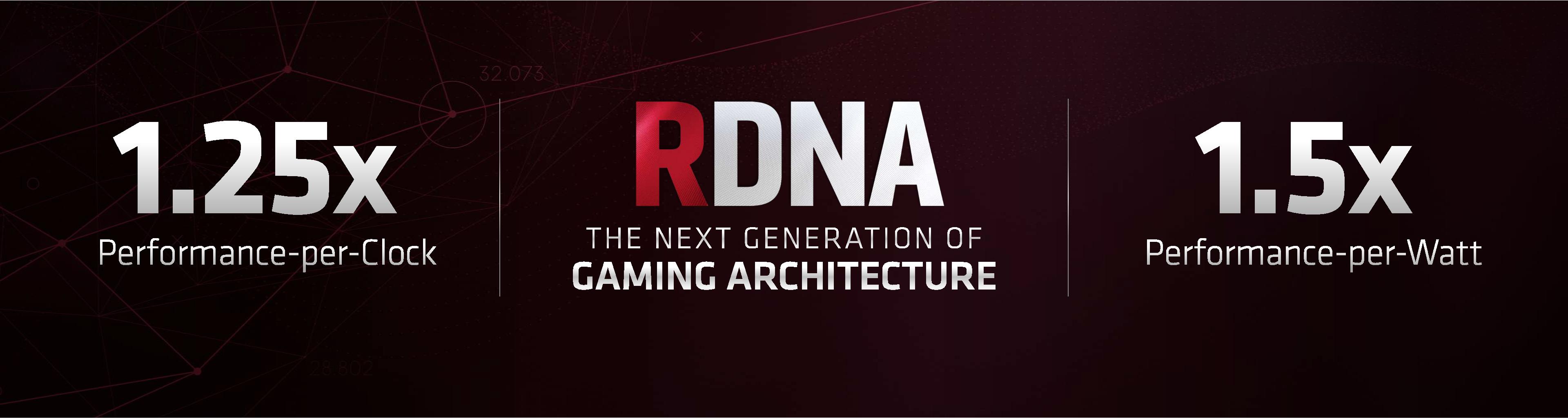
Wow impressive 2.8x. Navis 1.5x looks mediocre by comparisonI found some older slides for Polaris 10 14nm FinFET:
Im beginning to think this GCN-RDNA hybrid is the one to blame
But i was thinking 14->7nm is a bigger jump than 28nm->14nm. Will search for tsmc specs.
But it was still 6TP! vs 6.175TP that's what i've been pointing out. They managed to keep most of the floating `point performance, that has nothing to do with cache or memory bandwith.X1X has the advantage of higher mem bandwidth, altered memory pipeline, and twice the GPU cache as RX 480. It's evident from their actions that the honey was in the mem/cache config. Desktop Navi will have significant changes towards higher CU efficiency and improved multi-tiered cache. X1X's magic bullet doesn't exist this time, comparatively.
DeepEnigma
Gold Member
Let's stop all that talk... we want FACTS
Let's talk about that 14TF PS5.
Pfft, only in FP16. Snek is flexing the real girthy specs.
Wanted to post something I've calculated. With zen 2 clocked at 3.2Ghz, supporting AVX256, and 7 cores dedicated to games you still cant emulate ps3 games reliably. The cell was effectively an APU with SPUs doing floating point calculation like a gpu but at speeds far greater than the fastest GPU ever made. To emulate ps3 games you need a 3.2Ghz gpu or 8 cores dedicated to gaming. The cell was truly a beast in rendering considering that 15 years on (when the ps5 releases) we won't be able to reliably recreate its capabilities. That is bananas
LordOfChaos
Member
TSMC's CEO said the company has started volume production of its 7N+ process technology, DigitTimes reported on Friday. It is the company's first process node to use EUV on a few critical layers. The company says the yield is on par with 7nm
Now im thinking is very likely. Any comments anyone?
Fwiw
AMD's CTO Mark Papermaster tells us to expect a 25 percent increase in performance from the new process, but he reiterated to EETimes that the move to the new process is challenging.Papermaster also said that the move to EUV (extreme ultraviolet) manufacturing, which will come with the 7nm+ node, will only provide "modest" device performance opportunities. We've also seen similar statements from AMD's Forrest Norrod, so it might be best to keep expectations for significantly higher clocks in check.
AMD Ryzen 3000 Series CPUs: Rumors, Release Date, All We Know About Ryzen 3
We separate the rumors from the facts about AMD's upcoming Ryzen 3000 chips.
Since 7nm+ is only sprinkling in EUV on a few critical layers rather than whole cloth, it sounds like AMD is downplaying expectations for it. So for a price sensitive console, probably don't expect it. Even if yeilds are the same, it wouldn't make sense for TSMC to charge the same for two differently performing nodes.
Last edited:
SonGoku
Member
I don't get that, in a console every perf increase matters. All of it could be used towards increased density and reduced power consumption without increasing clocks or is 7nm+ much more expensive?Since 7nm+ is only sprinkling in EUV on a few critical layers rather than whole cloth, it sounds like AMD is downplaying expectations for it. So for a price sensitive console, probably don't expect it. Even if yeilds are the same, it wouldn't make sense for TSMC to charge the same for two differently performing nodes.
- Status
- Not open for further replies.