Pyramid Song
Member
Cerny's magic.lets speculate a bit. if both both MS and Sony have an APU with a similar CU count in what way can one be 25-30% more powerful?
Cerny's magic.lets speculate a bit. if both both MS and Sony have an APU with a similar CU count in what way can one be 25-30% more powerful?
"The combination of the S O C and the solid state drive.." (it does sound like SSD first time you hear it)
[2:06 timestamp]
What I don't understand is why MS is exclusively using people's moms and dads to describe the console .. I get that gamers are getting older, but bring back J Allard for christs sake - this is dull
PS5 Jetfighter Edition
Neither, because that 4chan post should not be taken seriously.lets speculate a bit. if both both MS and Sony have an APU with a similar CU count in what way can one be 25-30% more powerful?
Wow. They actually quote the same things Cerny told Wired, word by word. Impressive.Our goal is to get rid of those things, that's what we're after.
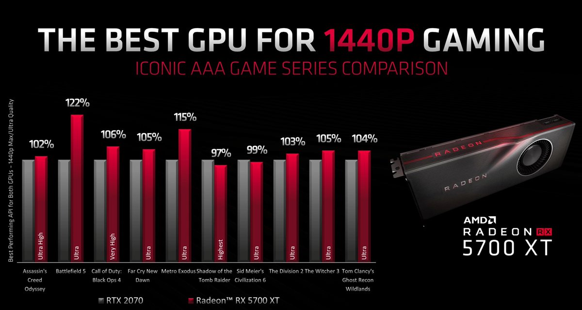
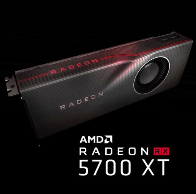
For people who think it will be 24 tflops
If you let me back I'll be here. Back to Scarlett... you mentioned it has four times the power of Xbox One X, which certainly sounds good. But what does that mean?
Matt Booty: It's a few things - it's the combination of speed, not just of the SSD but of the processor, the performance of the GPU and RAM, but we're also in a world where speed is starting not to matter. You can make RAM faster either by speeding up the way you access it or by adding more access points. Just think, what are all the things right now which take you out of a game? You're playing then suddenly *bloop* a load screen pops up and drops you out. Our goal is to get rid of those things, that's what we're after.
What do you think about the state of the industry right now? When you look around, who's here, who's not, what trends are you seeing in the industry?

The big Xbox interview - Project Scarlett, cross-gen Halo Infinite and the lack of Fable
Microsoft kicked off E3 in style today, with a memorable press conference that had Keanu Reeves and a car made out of L…www.eurogamer.net
I don't know why, but I've got a feeling Microsoft's console will be more advanced than Sony's.
Probably the X still gives them the advantange as it is the most powerful console today.
After the Azure partnership this wouldn't surprise me at all, but they're still playing chicken game with specs, so...Must be something like that..
Crazy thought: What if MS went to Sony (or vice versa): 'Hey, want to do splitsies on the SOC development for next gen?'. 'Yeah, good idea.. Then we could also use the same servers for cloud streaming.' and so on. Only difference being the software, the housing and the cooling obviously (Sony always fucks that one up.. Kinda like AMD). Would also be a dream for every third party developer.
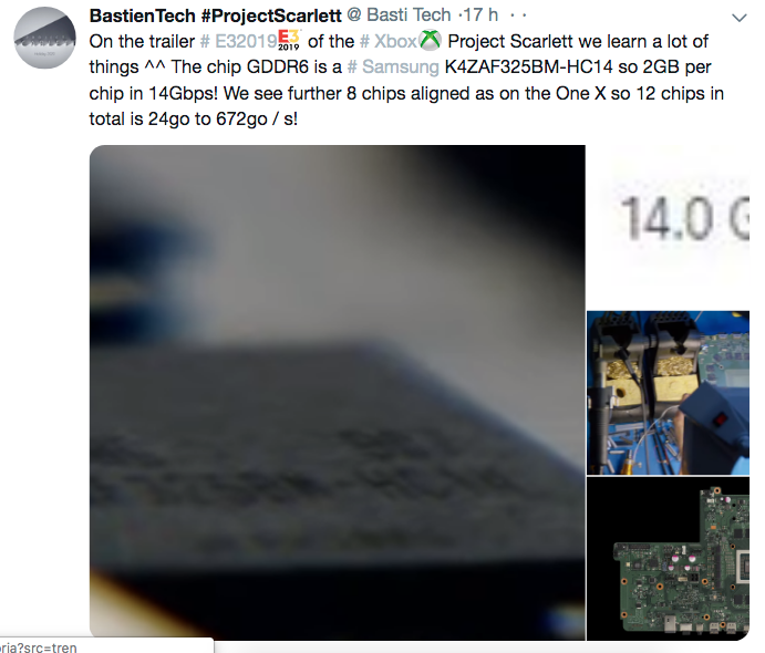
Another journalist saying the specs are basically locked at this point... maybe some changes in clock.
Cell2 literight but lets pretend the final SoC is similar, similar CU count no esram and all that. clock speeds are similar too. What magic sauce can one side use to be more powerful than the other?
I wonder if this was intentional or not. Now Sony can possibly use HC18 chips (if they really need it).24Gb of GDDR6 @ 672Gb/s CONFIRMED

[more] I spotted 12 (3 on each side) - at 2GB (16Gb) that's 24GB
[more 2] (so 674GB/s)
[edit] If I had the DRAM chip size the die size of the APU could be estimated - don't have it though..
Another journalist saying the specs are basically locked at this point... maybe some changes in clock.
Things like CPU cores, GPU CUs, amount of RAM chips are locked in, while clocks are still undecided. That's what he probably means.I see nothing of substance there. Pretty well locked in with flexibility is not locked in at all IMO.
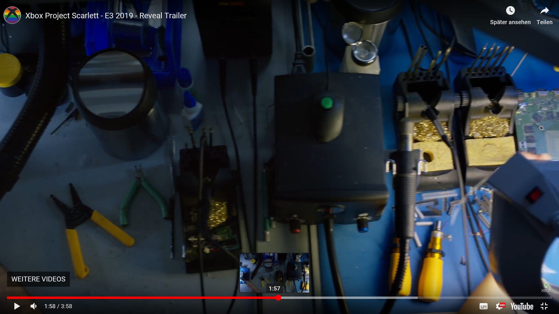
where did you spot 12? i didn't see more than two sides around the SOC.
concerning 3 packages on four sides i'm not sure that is even possible. you'd have to space your memory controllers in a manner on the soc that you have somewhat similar distances (or better bus lengths) between the ram packages and the memory controllers, otherwise V_drop won't be constant among them. you'd also have to leave space for your PCI4 bus on the SOC which would take enough space that you shouldn't be able to fit more than a max of 2 GDDR packages (at max) on this crtitical side.

Because we see it beat 2070 even in vidia sponsored games like OC Odissey?Yeap Radeon RX 5700 turned out lower than expected... it will probably lose most benchs to RTX 2070.

ok so there's something fuzzy off far right at ~1:16 - I think I can see 3 top, and at least 2 right .. so cofirmation bias + expections + logic (not 11) =12where did you spot 12? i didn't see more than two sides around the SOC.
concerning 3 packages on four sides i'm not sure that is even possible.
Beyond3D is saying there is two boards in the Scarlett video... one blue and another green.
The Blue motherboard has 12 GDDR6 chips while the Green has only 6 GDDR6 chips...
Lockhart (green) and Anaconda (blue)?
Beyond3D is saying there is two boards in the Scarlett video... one blue and another green.
The Blue motherboard has 12 GDDR6 chips while the Green has only 6 GDDR6 chips...
Lockhart (green) and Anaconda (blue)?
The green board is the Xbox One X. At least that's what it looks like to me.i can't see shit on the blue board in the video. and the green one could also house 12 packages
I'm reading a bit more in the thread some said one of the boards are literally the actual Xbox One X board... that one with 12 chips.i can't see shit on the blue board in the video. and the green one could also house 12 packages

The blue is Scarlett? You can see only 6 memory spots in that one.The green board is the Xbox One X. At least that's what it looks like to me.
i can't see shit on the blue board in the video. and the green one could also house 12 packages
The green board is the Xbox One X. At least that's what it looks like to me.
+1I'm reading a bit more in the thread some said one of the boards are literally the actual Xbox One X board... that one with 12 chips.
I'm reading a bit more in the thread some said one of the boards are literally the actual Xbox One X board... that one with 12 chips.

Next Generation Hardware Speculation with a Technical Spin [post E3 2019, pre GDC 2020] [XBSX, PS5]
The latest tensilica cores on 7nm can do 1.8 Tops, they doubled the perf per mm2 from the previous 14nm dsp core. Maybe they are going to have a few of those for audio, AI, and RT helpers.forum.beyond3d.com

yeah might really be x1x. but the pcb layout there is good for that type of memory configuration. could probably go with it.
Another journalist saying the specs are basically locked at this point... maybe some changes in clock.
Why would they use NAND storage as a GPU framebuffer (tons of read-write-modify operations)? I won't even mention the speed disparity (2-4 GB/s vs 672 GB/s).concerning the quote from the conference that the SSD now works more like an additional pool of RAM:
i think sony and microsoft both will go with an evolution of AMD's high bandwidth cache controller which allowed the user since vega to dedicate some part of his system RAM as addtional frame buffer (there have historically even been radeon instinct cards which let you put on a SSD as a VRAM extension). as soon as turned on, the game only see's one vram pool and the data micromanagement is done by the HBCC autonomously.
Why would they use NAND storage as a GPU framebuffer (tons of read-write-modify operations)? I won't even mention the speed disparity (2-4 GB/s vs 672 GB/s).
Next-gen consoles will most likely use QLC NAND (100-1000 write cycles) for cost reasons.
Already confirmed bu the Eurogamer article but let's post due the lack of leaks.
I still think manual micromanagement will be required to maximize efficiency. Automatic management is nice, but it yields much lower efficiency usually.the point of my post was not that they would use NAND as a framebuffer but that AMD has the technology to further unify memory pools in an "invisable to the user" manner (HBCC and as i posted some time ago storeMI for that matter). sorry if that wasn't comprehensible.
Because it is a thing... a big thing.LOL Ok. Good, I guess.
Why is anybody making this a thing?
I still think manual micromanagement will be required to maximize efficiency. Automatic management is nice, but it yields much lower efficiency usually.
That was also the case with eSRAM. MS has some tools to make it transparent to programmers, but I remember a DICE presentation about Battlefield arguing that manual programming is better.
yeah i bet your right about that. but i think it would be crucial that there was an "automatic mode" for accessibility for lower budget projects.
Already confirmed bu the Eurogamer article but let's post due the lack of leaks.
On Halo Infinite's official page it talks about Project Scarlett of 'consoles'. There is gonna be two SKUs.Code named 'Scarlett'
Anaconda DON'T exist
Scarlett is the codename to the next-gen platform or project.Code named 'Scarlett'
Anaconda DON'T exist
Scarlett is the codename to the next-gen platform or project.
Anaconda is the codename for one model of Scarlett.
Lockhart is suppose to the the codename of the other model of Scarlett.
MS is trying to dodge questions about Lockhart but it is clear that they have two Scarlett models to be launched... they said it last E3, they didn't deny in EG interview and they wrote again that in Halo Infinite official page.
I did not even cut off the changes for a 3rd model... the streaming only.
Ummm. Project Scarlet is the code name for their next gen project, and there are two SKUs under that umbrella:Maybe but the one they've shown is code named Scarlett.
So unless there's going to be three of them either Lockhart or Anaconda is no longer.
