• Hey, guest user. Hope you're enjoying NeoGAF! Have you considered registering for an account? Come join us and add your take to the daily discourse.

Next-Gen PS5 & XSX |OT| Console tEch threaD

Status
Not open for further replies.

SonGoku

Member
SSDs are basically arrays of NAND chips. The more flash chips you have, the faster the SSD is (assuming the controller can handle it).

A 2TB SSD is probably too much, even with late 2020 prices. 1TB will be the sweet spot and 2TB will be left for Pro models/future SKUs.
So like hbm then? the more stacks you have the faster you run
 

Ovech-King

Member
lol people stop comparing the 5700xt (or any previous Vega products for that matter) to next gen consoles. YES they are below 10TF but you seems to forget they only sports 8gb of GDDR6 ram
 

bitbydeath

Member
lol people stop comparing the 5700xt (or any previous Vega products for that matter) to next gen consoles. YES they are below 10TF but you seems to forget they only sports 8gb of GDDR6 ram

No Ray Tracing either.

If the below graph is any indication then we should be expecting next-gen to be modelled off Navi 21 as it’s much closer to the specs we currently know and expect.

izFaXrD.png
 
Last edited:

luca_29_bg

Member
Not really, seems to me people are going "10TF or bust" for either console. Navi or Vega, people dont care as long as its 10TF.

My personal opinion is that 12.9TF and "Almost 13TF dev kits" that Benji shared on twitter where related to Vega card used to emulate ~8.5TF Navi + hw RT that will be used in retail console but Sony obviously couldnt get chip out so early when dev kits where sent (January).

Mark Cerny said that sony sent kits out at the time of the wired interview, so i guess a second generation of kit.
 
lol people stop comparing the 5700xt (or any previous Vega products for that matter) to next gen consoles. YES they are below 10TF but you seems to forget they only sports 8gb of GDDR6 ram
Well, to be fair the PS4 GPU was a derivative of this:


Yeah, it was a laptop GPU, not the desktop 7850-7870 one.

Of course that doesn't mean that a 2020 console is going to follow the same strategy (cheap laptop parts, $399 MSRP), since lots of things have changed since 2013 (PSN profits, global economy).

SpinningBirdKick SpinningBirdKick

I think you're gonna like this one:


Evading a critical question like a true politician. :)
 
No Ray Tracing either.

If the below graph is any indication then we should be expecting next-gen to be modelled off Navi 21 as it’s much closer to the specs we currently know and expect.

izFaXrD.png
Won’t get Navi 21 be like 499 since it’s launching at 2020. Make sense to for consoles to go for Navi 10 since it will be cheaper by the release of Navi 21
 
Not informed about amd history but why didnt they go with 7nm before or 8nm? It seems weird that just recently they took advantage of this tech since I assume tmcn has been scaling down the size of these chips for a while now. LIke by 2021 the 6nm chips will be released followed by 5nm etc.
 

Imtjnotu

Member
Not informed about amd history but why didnt they go with 7nm before or 8nm? It seems weird that just recently they took advantage of this tech since I assume tmcn has been scaling down the size of these chips for a while now. LIke by 2021 the 6nm chips will be released followed by 5nm etc.
It doesn't really go down by a single mm every time. Somewhere between tsmc and Samsung there is some standard of sizes used. Gotta find the article I read this on
 

LordOfChaos

Member
Not informed about amd history but why didnt they go with 7nm before or 8nm? It seems weird that just recently they took advantage of this tech since I assume tmcn has been scaling down the size of these chips for a while now. LIke by 2021 the 6nm chips will be released followed by 5nm etc.

I'm not sure what your question is. AMD had the first consumer 7nm GPU out with Radeon VII.

TSMC 7nm is the most current volume node they have, 7nm+ and 6nm will be scaling up in volume. They couldn't use it earlier because it's a newish node, AMD was actually on the leading edge with it, apart from Apple who can pay for whatever leadership they want, and Huawei who was asking for a far smaller chip than any of these on it.
 
Last edited:
I'm not sure what your question is. AMD had the first consumer 7nm GPU out with Radeon VII.
I am trying to figure out how sony/ms will handle price, both consoles have great technology available now that can take game graphics to new heights and i dont want them avoid taking advantage of that by going for a cheaper machine for profit.

The theory is both can sell at 500 because a 6nm chip will be released in 2021 which will bring down the price i think. So I was wondering why didnt this happen before since i assume that tmnc was always scaling down the size of their chips.

It feels like something is special about this gen lol
 
Last edited:
TSCM was stuck on 28nm for years, 16nm was the first node reduction and that was 3 years after the PS4 launched
OHHHHHHH damn okay so i guess the theory is more paulisable than i thought since they are getting smaller much faster. I wonder what kind of breakthrough tech that broke them out of 28nm. Damn this upcoming gen really is special lol
 
Seems like Ps5 may end up being at ???Gb gddr6 18Gpbs since Scarlett seems to be visually confirmed 4 x 3 2gb chips so 24gb Gddr6 at 14Gbps

Just to quote the capabilities of 18Gbps chips from the web : "Samsung is now mass producing new GDDR6 memory uses 16 Gb dies (2 GB) featuring pin speeds of 18 Gbps (gigabits-per-second) and is able to hit data transfer speeds of up to 72 GB/s per chip."

Put Scarlett bandwidth at 672Gb/s
(54Gb/s per chip) and PS5 at either 576Gb/s if 16Gb ram or if we are lucky 864Gb/s at 24 Gb of ram ... That's a gap of about 30% (wink wink) between the two platform at 24 Gb of ram....!

Lisa Su said Cerny is planning the ps5 for the next ten years , it wouldn't surprise me if they go at 24gb


Like i said to SonGoku SonGoku few pages back, there are 2 different chip sizes noticed in video: 1 and 2 GB chip sizes because 2 different codes. So, highly likely it won't be 24 GB of RAM in new Xbox. This is post from other forum ( guy is a good poster and pretty reasonable member ) :

anapasteupq2jxq.png


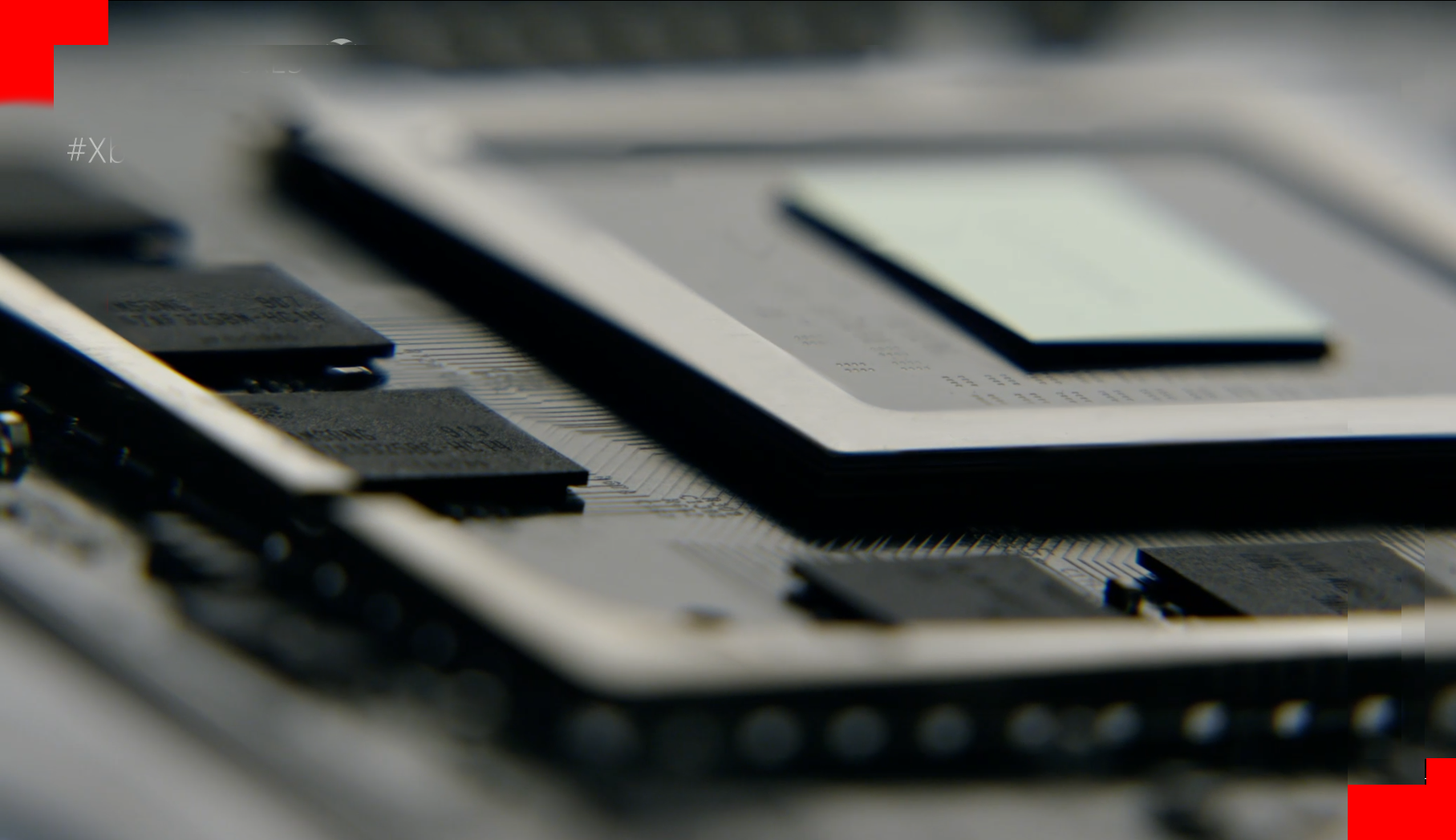
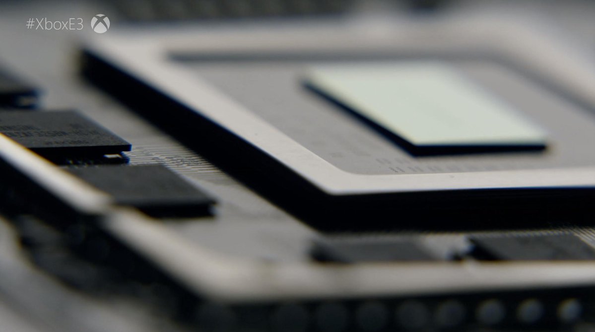
There's no paint-in here--that is, I didn't add any pixels. But obviously, I made choices about where and what to erase and combine, and my decisions may not have preserved accuracy. This image should definitely not be relied on for size measurement, counting of traces, etc.

But it's good for rough conclusions, and I think well demonstrates the evidence for a 320-bit memory interface. There are apparently no RAM chips on the far side, so all would be situated to the left, bottom, and (offscreen) the right of the APU package. The 3 chips on the left fit entirely within the length of the package. The 2 chips at the bottom start outside the package edge, and don't reach the center of the die. It would thus make most sense for there to be 4 chips total at bottom, with 2 offscreen. Logically, there'd then be another 3 chips on the right. Though they can't be seen, the view past the top-right package corner shows no RAM in a corner position...and further down at the very edge, there's a mild dark blur that could be out-of-focus RAM in the expected position.

This adds up to very good evidence for 10 RAM chips in a 3-4-3 configuration. At 32-bit per GDDR6 chip, that's a 320-bit bus. Given 14bps chips (see below), total RAM bandwidth would be 560GB/s. That's about 72% higher than Xbox One X; it's 25% higher than both the new Navi GPUs and the Nvidia RTX 2080 (though in Anaconda this would be shared with the CPU).

As for size, two different Samsung designations can be seen. The middle chip on the left, and probably the right one at bottom, are code 325BM-HC14. This is 16Gb/2GB capacity and 14Gbps speed. The lower chip on the left is code 325BC-HC14, an 8Gb/1GB capacity at the same speed. Presuming symmetry of the left with the proposed unseen chips on the right, we have 10GB known, plus 4 unknown chips. That'd allow 14, 16, or 18GB total.

Hopefully this is helpful for folks that hadn't seen this data fully explicated before. Note that apart from the newly enhanced image, none of this analysis is new from me. It was developed by others earlier, notably @DukeBlueBall . But I believe a thorough layout like this will show that the memory bandwidth and (in a tight range) amount are probably known for Anaconda, even though not verbally announced by Microsoft.


THE:MILKMAN

Member
Call me crazy but I still think that Scarlett board above is some sort of test or pre-production board versus a render. I can't see why Microsoft would go to such trouble to render a QR code and real life model numbers for a third-party product.

The most interesting thing as said above is the mixed density chips and whether that is just for testing purposes or if some sort of compromise around bus width/RAM or power?

Just for a point of comparison below is the Subor Z board that is said to contain a APU around 390mm^2 and of course has 8 GDDR5 chips:

feng.JPG
 

Evilms

Banned
Like i said to SonGoku SonGoku few pages back, there are 2 different chip sizes noticed in video: 1 and 2 GB chip sizes because 2 different codes. So, highly likely it won't be 24 GB of RAM in new Xbox. This is post from other forum ( guy is a good poster and pretty reasonable member ) :


D8plNBWUYAA4EAY.jpg


We can read in the picture 4ZAF325BM-HC14 maybe K4ZAF325BM-HC14 (Samsung), The Scarlett it's probably going to be a 12 x 2 Gb configuration for 24 Gb memory and with 384-bit bus (32-bit per 2 Gb chip).

Xda1uUb.jpg
 
Last edited:
D8plNBWUYAA4EAY.jpg


We can read in the picture 4ZAF325BM-HC14 maybe K4ZAF325BM-HC14, The Scarlett it's probably going to be a 12 x 2 Gb configuration for 24 Gb memory and with 320-bit bus (32-bit per 2 Gb chip).

Xda1uUb.jpg

Looks like you missed the picture in my previous post where are 2, CLEARLY visible, different memory codes

"The middle chip on the left, and probably the right one at bottom, are code 325BM-HC14. This is 16Gb/2GB capacity and 14Gbps speed. The lower chip on the left is code 325BC-HC14, an 8Gb/1GB capacity at the same speed. "

So, it's not a 24 GB at all. It's should be a range from 16-20 GB
 
Last edited:

Evilms

Banned
Looks like you missed the picture in my previous post where are 2, CLEARLY visible, different memory codes

"The middle chip on the left, and probably the right one at bottom, are code 325BM-HC14. This is 16Gb/2GB capacity and 14Gbps speed. The lower chip on the left is code 325BC-HC14, an 8Gb/1GB capacity at the same speed. "

So, it's not a 24 GB at all. It's should be a range from 16-20 GB

If so, it would be a surprising choice, which means we'll have a 3-4-3 config instead of the 4-4-4 like on the X, strange.
Honestly 16 Gb of memory I find it very low for a next gen console.
 
If so, it would be a surprising choice, which means we'll have a 3-4-3 config instead of the 4-4-4 like on the X, strange.
Honestly 16 Gb of memory I find it very low for a next gen console.

Nvm.

Anyway, 16 GB with high bandwidth maybe should be enough?

Even 2080 TI doesn't have that much
 
Last edited:

xool

Member
"The middle chip on the left, and probably the right one at bottom, are code 325BM-HC14. This is 16Gb/2GB capacity and 14Gbps speed. The lower chip on the left is code 325BC-HC14, an 8Gb/1GB capacity at the same speed. "

ok - from the reveal video (you might need to open each image separately)

  1. clearly ends 325BM-HC14
  2. probably BC-HC14 (fuzzy in all images)
  3. there's something on the far and far-top sides - could be three more RAM chips each, ro something else
 

-kb-

Member
ok - from the reveal video (you might need to open each image separately)

  1. clearly ends 325BM-HC14
  2. probably BC-HC14 (fuzzy in all images)
  3. there's something on the far and far-top sides - could be three more RAM chips each, ro something else


The row in the top back (furtherest from the viewer) doesn't look like it has sufficient gaps between it to be more memory modules like the three other sides (bottom, left and right). I have a feeling its VRMs.

You can see something similar on the left side of the APU on this XB1X motherboard shot.

 
Last edited:

xool

Member
The row in the top back (furtherest from the viewer) doesn't look like it has sufficient gaps between it to be more memory modules like the three other sides (bottom, left and right). I have a feeling its VRMs.

You can see something similar on the left side of the APU on this XB1X motherboard shot.


Makes sense
 

TeamGhobad

Banned
Looks like you missed the picture in my previous post where are 2, CLEARLY visible, different memory codes

"The middle chip on the left, and probably the right one at bottom, are code 325BM-HC14. This is 16Gb/2GB capacity and 14Gbps speed. The lower chip on the left is code 325BC-HC14, an 8Gb/1GB capacity at the same speed. "

So, it's not a 24 GB at all. It's should be a range from 16-20 GB

why would they mix like that? why not just use 2gb chips? cost? heat? i doubt it costs that much more to have 2 gb chip than a 1gb..
 

R600

Banned
I assume its heat related. Obviously, this setup gives them headroom to match anything competition does, as replacing GDDR chips is probably easiest thing to replace 1.5yr before release.

I guess MS is open to 16-20GB variant - 560 GB/s at 320 bit bus.

This is what I predicted. One advantage of GDDR6 v HBM2 is single pool of fast memory that is modular enough to give you headroom to increase amount of memory you have based on what competition is doing. With HBM2 this is much harder to do.
 
Last edited:

nowhat

Member
we're talking dollars here...
Dollars don't use a linear scale? Some of the costs are constant. But if a 1GB chip is x dollars, a 2GB chip will be ~2x dollars. Depending on the price of a GB (and the price target for a console), the difference may be significant.
 

TeamGhobad

Banned
Dollars don't use a linear scale? Some of the costs are constant. But if a 1GB chip is x dollars, a 2GB chip will be ~2x dollars. Depending on the price of a GB (and the price target for a console), the difference may be significant.

2gb chip isnt twice the price

I assume its heat related. Obviously, this setup gives them headroom to match anything competition does, as replacing GDDR chips is probably easiest thing to replace 1.5yr before release.

I guess MS is open to 16-20GB variant - 560 GB/s at 320 bit bus.

This is what I predicted. One advantage of GDDR6 v HBM2 is single pool of fast memory that is modular enough to give you headroom to increase amount of memory you have based on what competition is doing. With HBM2 this is much harder to do.

the bus will be 384-bit though they arent lowering it from scorpio. they might even increase it, who knows. if MS can't compete on tflops they might compete on ram instead.
 
Last edited:

R600

Banned
the bus will be 384-bit though they arent lowering it from scorpio. they might even increase it, who knows. if MS can't compete on tflops they might compete on ram instead.
Its all about requirements and heat/price. If 20GB @560GB is enough for ~9TF + Zen2, thats what they will use. No use to have more BW if GPU and CPU does not require it. 14Gbps @ 384 bit bus is 672 GB/s, I think too much and also cant see a system with that BW and die size (~390mm2) getting beaten by anything from Sony if they are not going for heavy loss/price increase.
 
Last edited:

xool

Member
why would they mix like that? why not just use 2gb chips? cost? heat? i doubt it costs that much more to have 2 gb chip than a 1gb..

Maybe this relates to the 2 SKU thing - they could use the same board for both, and swap 1GB chips for 2GB in the higher specced machine etc..

..haven't really thought this through - I suspect there would be gotchas with this plan
 

jonnyp

Member
Dont see why the doubt for SSD. Mark cerny himself stated it would be the fast SSD so far and their goal is to have seamless experience. I dont see the benifit in outright lying, maybe if he used vague language to describe the SSD i would agree but to directly state its the fastest is something else imo

You didn't read my posts. I never said it won't have an SSD. I'm saying I don't think it willl be 1TB.
 
No, RAM chips are placed around SOC. It adds to motherboard complexity, but not die size of actual chip.
Ok, I got you. But what is that secondary ring around the RAM, the primary being the SOC itself? I wonder if that entire section is modular, allowing Microsoft to upgrade/downgrade at minimal cost.
 
Last edited:

LordOfChaos

Member
OHHHHHHH damn okay so i guess the theory is more paulisable than i thought since they are getting smaller much faster. I wonder what kind of breakthrough tech that broke them out of 28nm. Damn this upcoming gen really is special lol

28nm was a brutal wait to get by, but the current change in pace is kinda driven more by naming.

7nm+ is 7nm with EUV on 4 layers. 6nm is 7nm with EUV on 5 layers. 5nm is with EUV on all 14 layers...

28nm was a freak but we're more just back to regular slowing fab updates, rather than getting faster.

If this was Intel we may have been joking about 7nm++++. Fab naming is complete marketing bullshit lol, so one should always look at the actual density.
 
Last edited:

SonGoku

Member
Like i said to SonGoku SonGoku few pages back, there are 2 different chip sizes noticed in video: 1 and 2 GB chip sizes because 2 different codes. So, highly likely it won't be 24 GB of RAM in new Xbox. This is post from other forum ( guy is a good poster and pretty reasonable member ) :
The use of different sizes chips is suspect to say the least, has there even been a gpu with asymmetric memory chips config?
2GB chips are supposed to replace 1GB, costs won't be much higher to justify this config

Proelite Proelite You are welcome to chip in :)
 
Last edited:
Status
Not open for further replies.
Top Bottom