I made a die shot analysis video for the Xbox Series X and S chips, though the first part is just limited to the I/O:
It may be interesting for some, especially since all sources are in the description box and I lay down how you can figure out different hardware blocks.
So to some extend it's like a tutorial and you can learn how to analyse die shots yourself.
However you need some background knowledge and not everything will be easy to follow if you are just a casual hardware enthusiast.
That said some may not like to watch videos or can't, so here is a small summary:
1.) When companies share the die sizes it's not always clear what they mean by that.
Sometimes they mean the whole chip size, sometimes just the chip design itself, without the scribe line.
In some cases the official die size doesn't fit either way, so the first thing you should do, when you want to measure structure sizes, is to check on the die sizes yourself.
https://abload.de/img/mega-leaks-part-5-xboyyjr3.png
2.) First a short CPU analysis of the Zen2 Matisse (CPU) and Renoir (APU) die shots.
They both share the same CPU core sizes of 2.83mm² and the structures look basically identical, so AMD uses the same design libraries and physical implementation.
https://abload.de/img/mega-leaks-part-5-xbok9jvo.png
3.) AMD only changed the L3$ design, reducing the capacity from 16MiB (CPU) to 4MiB (APU).The CCX size goes down from 31.37mm² to 20.21mm².
A Renoir CCX is 11.16mm² smaller.
You could get 3x 4MB CCXes (3x 20.21mm = 60.63mm²) for the price of 2x 16MB CCXes (2x 31.37mm² = 62.74mm²).
It's more than obvious why there is a large motivation in cutting down the L3$ if area is important.
https://abload.de/img/mega-leaks-part-5-xbo5ojye.png
4.) In the past I made a hypothetical CCX mockup with 8MB per CCX, resulting in ~24.23mm².
It was an interesting question what Renoir, the Xbox Series and PS5 would use (was still open back then).
Now it's known that Renoir, Xbox Series and PS5 all use 4MB for the L3$ per CCX.
https://abload.de/img/mega-leaks-part-5-xboeckzt.png
5.) The assumption now is of course that the Xbox Series and PS5 use the same Renoir design and implementation (which is not true for the PS5 as we know).
Comparing the Xbox Series CCXes to AMD's Zen2 CCXes shows basically the same picture, at least the size should be identical.
https://abload.de/img/mega-leaks-part-5-xboh9j0c.pnghttps://abload.de/img/mega-leaks-part-5-xborkk9d.png
Because of the low resolution it's hard to tell if some digital logic is not laid down differently, on the FPU and L3$ side there appear to be some differences but I wouldn't make the call right now.
6.) The core size on the Xbox Series should be identical with 2.83mm², meaning the die shot MS shared at Hot Chips is 372.16mm², larger than the final chips.
https://abload.de/img/mega-leaks-part-5-xbo07jqp.png
7.) Thanks to the XSX teardown on ifixit we can say that the final chips are ~360mm² in size, as MS officially stated with 360.45mm².
The chip design itself is ~354.71mm² large on XSX and 192.18mm² on the XSS.
https://pbs.twimg.com/media/Ew2ziieWgAsA8Z8?format=jpg&name=large
https://abload.de/img/mega-leaks-part-5-xboeakmw.png
https://abload.de/img/mega-leaks-part-5-xbonrjsg.png
8.) For time reasons I just managed to include the I/O sections, where MS is stating 5 I/O blocks, 3 on the left and two on the right side.
We obviously want to know what they are for.
Looking at them makes it clear that we have two different types of I/O.
Based on official information we only have 3 major I/O connections; Display, 8x PCIe4 Lanes and GDDR6 links.
2x PCIe4 lanes are used for the internal and 2x for the external SSD.
The Southbridge is a dedicated chip which is also attached via the PCIe standard and contains USB3 interfaces, a system controller, SPI, etc.
So one I/O type should be for display and the other for PCIe.
The left I/O blocks don't fit to 4 display links or 8 PCIe4 lanes.
But the right I/O blocks have 4 yellow stripes and if those are PCIe Lanes that would fit perfectly to 8 PCIe4 Lanes.
https://abload.de/img/mega-leaks-part-5-xboz6khw.png
9.) We can check that simple assumption thanks to Fritzchens Fritz, who has die shots of Navi10 and Navi14 on his flickr account.
Comparing the I/O sections and other analog elements shows basically no differences, outside of two larger blocks colored in red and cyan.
N10 has 6 red blocks, N14 just 5.
N10 has 4 cyan blocks, N14 just 2.
https://abload.de/img/mega-leaks-part-5-xboickrc.png
10.) The cyan blocks look identical to the right I/O blocks on the Xbox Series X and they share the exact same size.
There is only one major I/O specification which could come into question here.
N10 has 16x PCIe4 lanes, while N14 only has 8x PCIe4 Lanes.
We can conclude that the cyan blocks are PHYs for PCIe4 and that each yellow stripe is a single lane:
https://abload.de/img/mega-leaks-part-5-xbomrjd7.png
11.) Finding the display specifications per GPU is not so easy, I think you really have to look at the open source drivers to find the information about how many display controllers are present per GPU.
N10 has 6, N14 5, which fits to the red blocks which look very similar to the left I/O blocks on Xbox Series.
https://abload.de/img/mega-leaks-part-5-xbo9sjo5.png
12.) Why the Xbox Series X has 3 of those (display) I/O PHYs is still a mystery to me, the Xbox Series S just has 1.
https://pbs.twimg.com/media/Ew25RAQWQAAtdwX?format=jpg&name=large
13.) One could also look at the traces on the PCB to figure out the I/O situation but for a layperson this is not always presenting a clear picture.
https://abload.de/img/mega-leaks-part-5-xboeckfu.png
14.) Finally the GDDR6 I/O, which MS officially annotated but they would have been easy to make out anyway.
DRAM PHYs are usually the largest interfaces on a chip and in most cases there are no other options which fit to the memory specifications.
For example the Xbox Series X has a 320-Bit wide interface and each GDDR6 memory chip is connected via 32-Bits, meaning that the PHY needs to fit to the number 10 in some way.
Either we should see 5 larger blocks, 10 or 20 but not something which is not part of that number series.
On the Xbox Series X we see exactly 10 larger I/O PHYs around the chip edges.
In addition I made just a visual representation how the 10GB of "GPU Optimal Memory" should be in principle mapped over the full 320-Bit Interface and how the 6GB "Standard Memory" is addressed over 192-Bits/6 memory chips.
https://abload.de/img/mega-leaks-part-5-xbodekll.png
https://abload.de/img/mega-leaks-part-5-xboy7jki.png
https://abload.de/img/mega-leaks-part-5-xbo83kyk.png
------
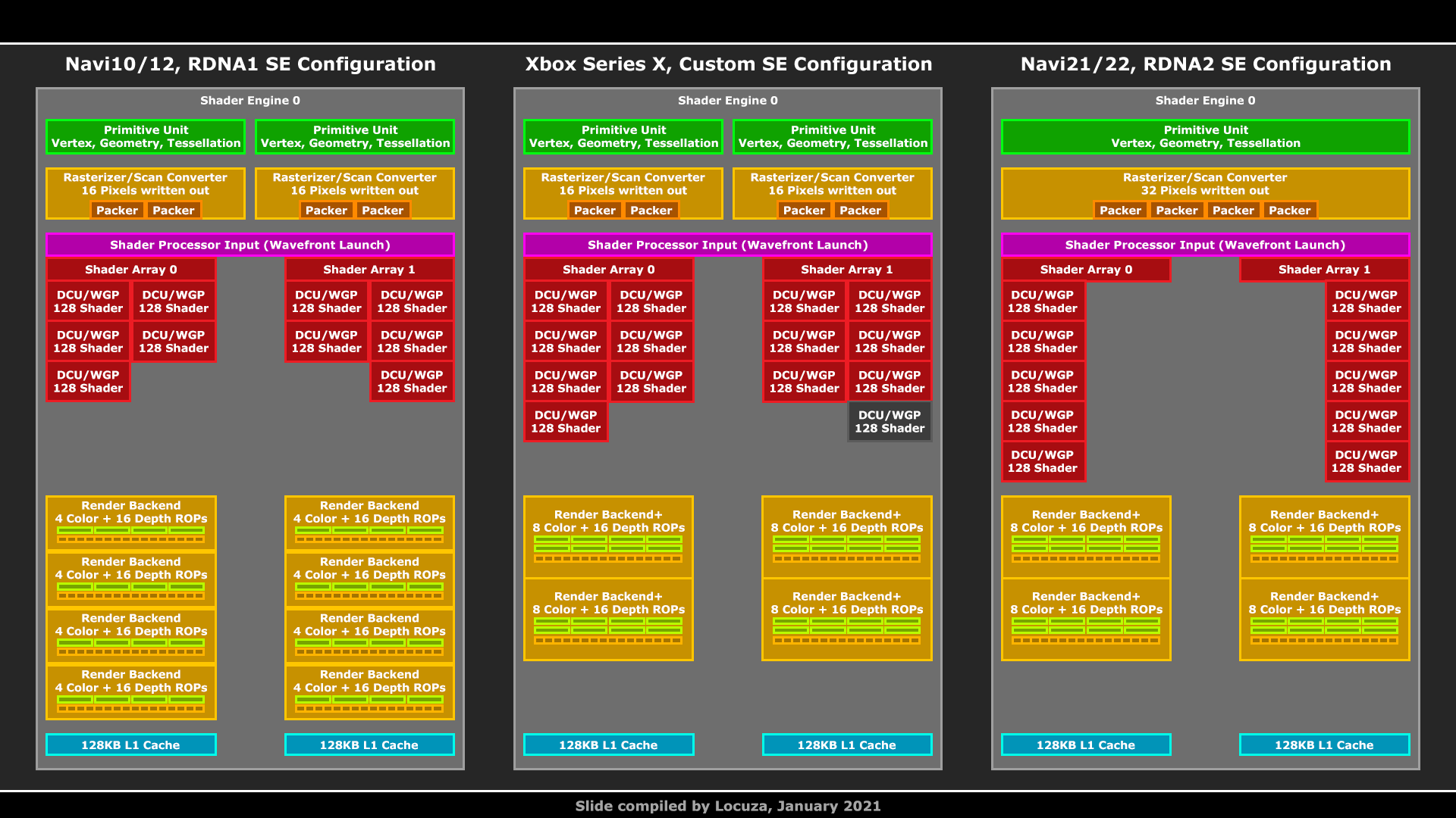
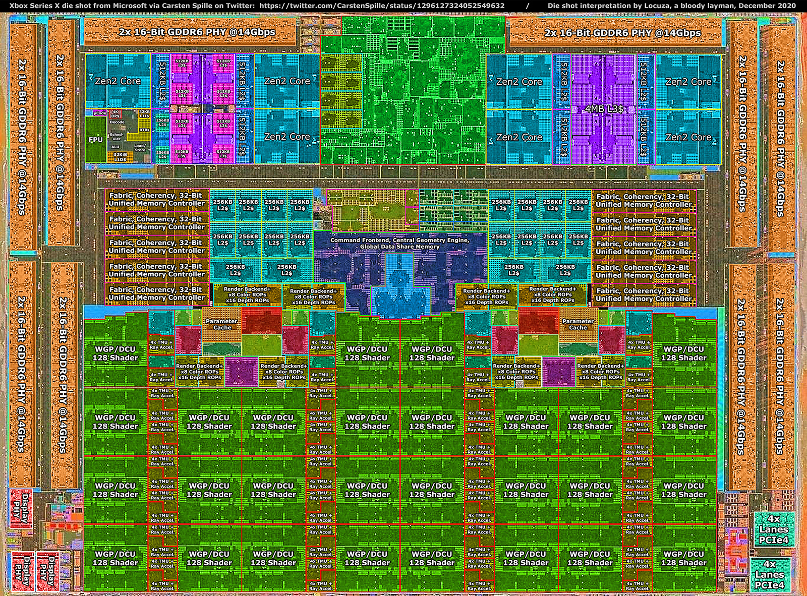
In the end we should roughly come up with this picture (yellow TMU blocks are part of the WGPs and the green/cyan blocks on the left and right side from the Parameter Cache should relate to the Primitive Units and Rasterizer):
Full res and with other information here:
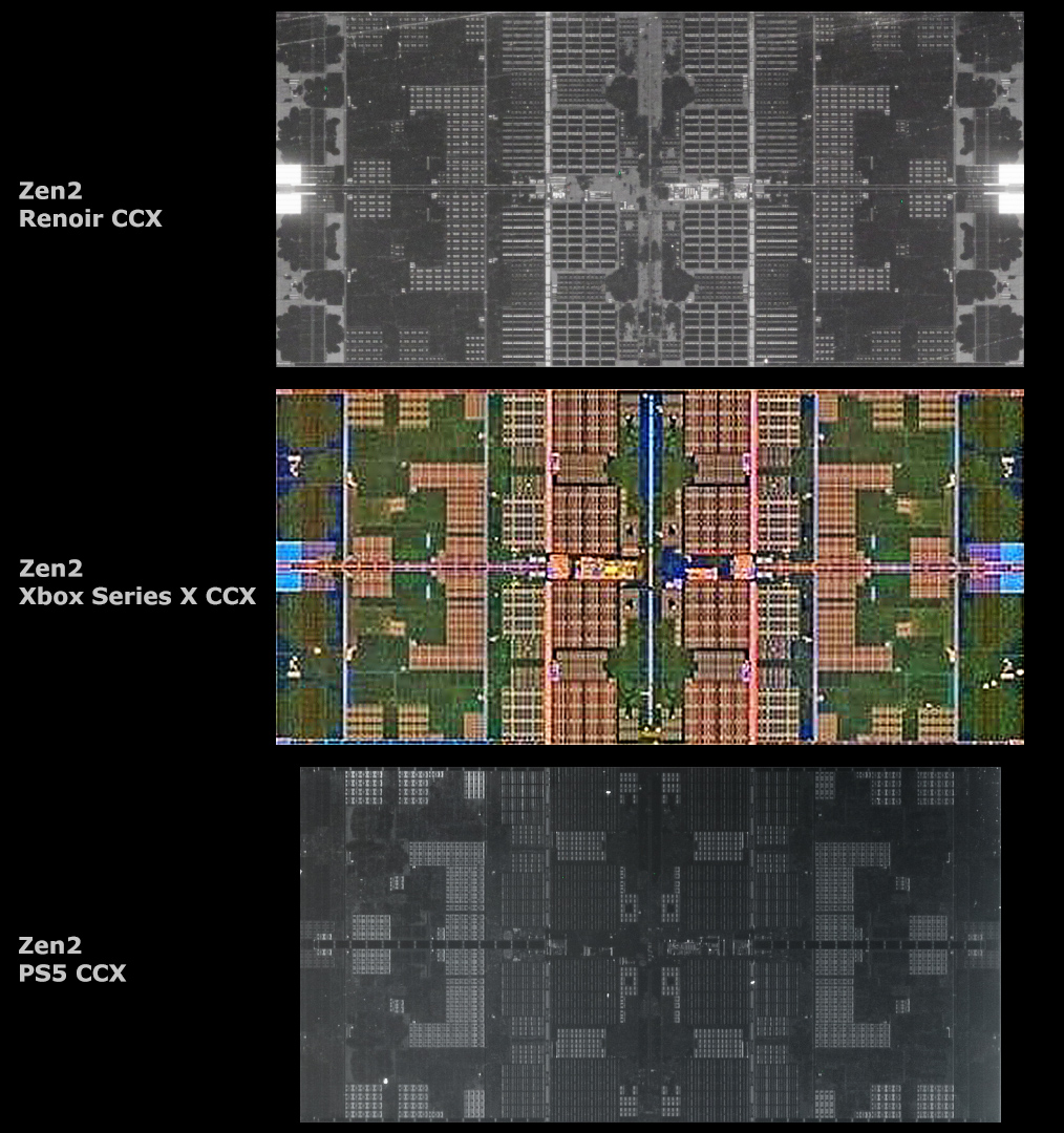
One interesting point may relate to the CCXes:
The PS5 CPU has some cut downs on the FPU side (at least the FP register file was reduced), making the CCX shorter than on the Xbox Series and AMD's Zen2 CPUs.
____
Any feedback, questions or answers are welcomed.


