• Hey, guest user. Hope you're enjoying NeoGAF! Have you considered registering for an account? Come join us and add your take to the daily discourse.

PS6 Specs you expect?

ap_puff

Member
That's why I said 5nm + 2nm chiplets.
Having half the chip on 2nm is cheaper than having the whole chip on 2nm.

I don't think the AI bloom would affect Sony tbh. Sony would be ordering 100+ chips, TSMC isn't going to panic, not one bit.
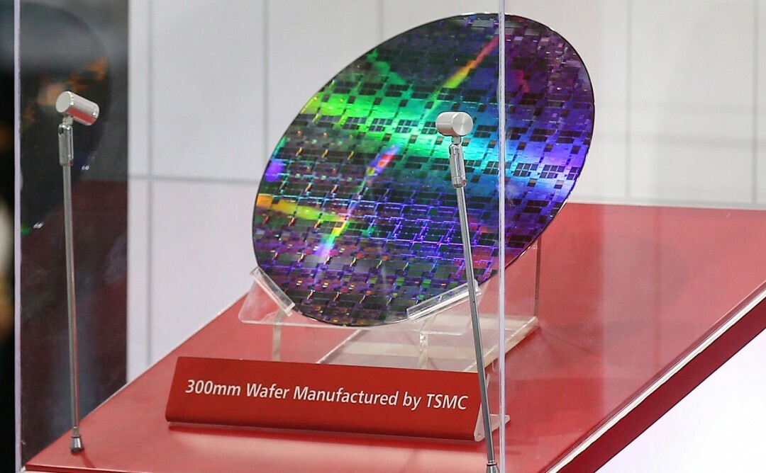
"However, TSMC is signaling potential shortages in leading-edge capacity to encourage customers to secure their allocations. Adding to the industry's challenges, advanced chip-on-wafer-on-substrate (CoWoS) packaging prices are expected to rise by 20% over the next two years, following previous increases in 2022 and 2023. TSMC aims to boost its gross margin to 53-54% by 2025, anticipating that customers will absorb these additional costs. The impact of these price hikes on end-user products remains uncertain."

Even the 5nm node is getting more expensive rather than trending downward

pANZ5H3.jpeg
 

Loxus

Member

"However, TSMC is signaling potential shortages in leading-edge capacity to encourage customers to secure their allocations. Adding to the industry's challenges, advanced chip-on-wafer-on-substrate (CoWoS) packaging prices are expected to rise by 20% over the next two years, following previous increases in 2022 and 2023. TSMC aims to boost its gross margin to 53-54% by 2025, anticipating that customers will absorb these additional costs. The impact of these price hikes on end-user products remains uncertain."

Even the 5nm node is getting more expensive rather than trending downward

pANZ5H3.jpeg
They're not going to charge those prices for Sony. Those prices are only going to affect the data center clients.
AMD HPC Solutions

Also, why would the PS6 use CoWoS?
 
Nodes get cheaper overtime.
Example.

They can go the chiplet route, 5nm + 2nm for example.

16nm might be cheaper, but 5nm is nearly twice as expensive as 7nm.
Problem is, microarchitectures are designed with a node in mind. You can't backport RDNA6 to 5nm without incurring massive costs in photomask design, as well as penalties in performance characteristics (power, frequency, die size etc).
So yeah maybe 5nm will be cheap when the PS6 launches, but that node will be two generations old at that point.

They're not going to charge those prices for Sony. Those prices are only going to affect the data center clients.
AMD HPC Solutions
How do you know what they're going to be charging Sony? Why would they sell any wafers to Sony, if they could get more money selling them to Nvidia or Intel or Ampere or whomever instead?

Also, why would the PS6 use CoWoS?
If they intend on using chiplets, then they'll need to use packaging technologies.
Chiplets might be the only way to avoid the cost of huge monolithic dies.
 
Last edited:

ap_puff

Member
They're not going to charge those prices for Sony. Those prices are only going to affect the data center clients.
AMD HPC Solutions

Also, why would the PS6 use CoWoS?
didn't you just say they would use 5nm + 2nm chiplets? that would require advanced packaging unless you just want some really gnarly latency penalties.
 

Diddy X

Member
With the direction things are heading I think next-gen is likely gonna suck big time,

-long-ass dev cycles (5+ years?)
-no innovation because too risky
-all remakes or safe bets
-MTX EVERYWHERE
-woke stuff (there is hope on this tho)
-expensive af hardware


I have absolutely no desire for a new console generation.
 
Assuming Xbox actually launches a next gen console in 2026 it's safe to safe we'll get a PS6 by 2027/28 which is only 3/4 years away.

So with the PS6 looming over the horizon and the PS5 Pro specs revealed what sort of horsepower do you expect the PS6 to have?
"Only"

Are people so desperate for the next big thing that they need to imply that 3-4 years is somehow a short period of time now.
 

Panajev2001a

GAF's Pleasant Genius
This is my idea.
Chiplet design with a 3 SED, 1 CCD and a I/O die.
A chiplet design means we can have a Base and Pro PS6 day one.

sFPpBlx.png


This is assuming PS6 is scheduled for a 2027 release.
Zen6 and RDNA5 are rumored for 2026-2027.
TSMC N2 is also scheduled for a 2026-2027 release.

UDNA is not needed for console gaming as that is design for cloud-to-client.

With the console most likely going full AI with Path Tracing, HBM4 with it high bandwidth maybe possible because it removes the expensive interposer in favor of 3D stacking.

Moving the SSD controller to the I/O to possibly remove PCIe bottlenecks and improve latency, that way we may possibly see split second loads.

Chip would be cooled utilizing Sony double sided heatsink patent.

Die sizes are 90% accurate as I used AutoCAD to scale Strix Point die shot to 2nm.
I would update this when PS5 Pro and RDNA4 die shot is available and as most fascinating tech is released.
Interesting you do not see them pushing for any dedicated extra AI HW, but they could extend what they have now. Going from 60 to 120 CUs seems an almighty big growth. Aren’t we estimating they would use a too new manufacturing node for Sony? We will see what they have used for PS5 Pro compared to expectations (Zen4c vs Zen 2 was one, but the manufacturing node was another one… I am also curious if this is really a new GPU arch or if they added more RDNA2 CUs with RDNA4 customised RT units and RDNA3.x ROPS… biggest news is that the ROPS now support VRR tier 2 as well so it may as well be RDNA2 ones… AMD did already do a node shrink of Zen 2 and Sony’s custom RDNA2 based GPU… oh well, you are right let’s wait for a nice PS5 Pro die shot :)!).
 

ap_puff

Member
Interesting you do not see them pushing for any dedicated extra AI HW, but they could extend what they have now. Going from 60 to 120 CUs seems an almighty big growth. Aren’t we estimating they would use a too new manufacturing node for Sony? We will see what they have used for PS5 Pro compared to expectations (Zen4c vs Zen 2 was one, but the manufacturing node was another one… I am also curious if this is really a new GPU arch or if they added more RDNA2 CUs with RDNA4 customised RT units and RDNA3.x ROPS… biggest news is that the ROPS now support VRR tier 2 as well so it may as well be RDNA2 ones… AMD did already do a node shrink of Zen 2 and Sony’s custom RDNA2 based GPU… oh well, you are right let’s wait for a nice PS5 Pro die shot :)!).
That mockup is also highly unrealistic. Hbm4? Lol that's never going in consumer grade hardware, especially not a console that's going to be sold at <$1k. HBM4 is going to be cutting edge and EXTREMELY expensive, hbm is still in high demand and multiple times more expensive than GDDR (which is why you don't see it in gaming GPUs, along with increased latency). Hell HBM3/E is basically only used by top end data center AI training hardware that costs $20,000-40,000+ per GPU, and most server grade stuff is still using hbm2.
 
Last edited:
CPU I say go with a Zen 6 with 3D V-Cache. 8c/16t should still be fine.

24 - 32GB of Ram at 1000+ GB/s memory bandwidth

Improve PSSR to DLSS 3.0+ levels

RDNA 5 - 6 GPU with 6x - 10x the Ray Tracing capablilties and at least 6x raw GPU performance over base PS5.

Improved SSD Read/Write Speeds. They will cheap out and probably release with only 2 TB drive.

$599 - $699
 
Last edited:

Trilobit

Gold Member
Assuming Xbox actually launches a next gen console in 2026 it's safe to safe we'll get a PS6 by 2027/28 which is only 3/4 years away.

So with the PS6 looming over the horizon and the PS5 Pro specs revealed what sort of horsepower do you expect the PS6 to have?

I just hope that we'll still be getting crossgen games with PS4 when PS6 is launched.
 

Zathalus

Member
- Whatever the best or second best CPU is from AMD, it will have cut down cache and no 3D cache either. 8-12 cores seems likely.
- GPU will again be custom version of the latest AMD architecture, I’m assuming 4090 +- 20% performance.
- GDDR7, around 1TB/s total bandwidth.
- Upgraded SSD.
 

peish

Member
If ps5 pro is a success, gamers will accept $599 for a next gen console. This is good news, Sony can use more special sauces like 3D cache and HBM.

Everyone, do your part and make PS5 Pro a word of mouth success.
 

hlm666

Member
They're not going to charge those prices for Sony. Those prices are only going to affect the data center clients.
AMD HPC Solutions

Also, why would the PS6 use CoWoS?
Sony don't buy the wafer, AMD do and sell the final product to Sony. No one but AMD can make their x86 chips because of the way the way the license from intel works.
 
Last edited:
- AMD Custom 12-core cpu
- custom RDNA6+/UDNA6, MCD and Obviously more CUs than PS5 Pro.
- 2X - 4X RT
- PSSR 2.0
- improved I/O
- 2TB pcie 5.0 nvme ssd, 12+ GB/s raw
- 32GB GDDR7, 1+ TB/s
- Tempest 3D 2.0
 
Assuming Xbox actually launches a next gen console in 2026 it's safe to safe we'll get a PS6 by 2027/28 which is only 3/4 years away.

So with the PS6 looming over the horizon and the PS5 Pro specs revealed what sort of horsepower do you expect the PS6 to have?
It's obvious it's going to be AMD again because Sony depends on them for hardware back compatible. Since it'll launch I'm 2028 according to what MS and Sony have said that means at most it'll run on Zen 6(launches 2026) and RDNA6 (2028) in practice it'll be RDNA 5.5 like the Pro is 3.5 and like the PS5 is 1.5. It won't be Zen 7 because Sony never uses the latest CPU arch see PS4 and PS5. It'll probably use smaller cores that are space efficient like Zen 4C cores in this case Zen 6C mixed in with regular Zen 6.

Hopefully by RDNA6 AMD will have caught up to Nvidia's 40 series so it'll have dedicated hw for RT, AI upscaling, path tracing and frame generation. AMD is not an innovator they always late so expect whatever Nvidia puts in their 50 or 60 series to go into RDNA6.

Next gen will be able to handle full fat RT like the 2080ti could in 2018, it will also be able to handle Path Tracing like the 30 series could in 2020 and advanced ai features like Ray reconstruction. Other than RT, path tracing and AI there's nothing else at the cutting edge so that will probably be it.
 

Gubaldo

Neo Member
Zen 2 - with higher clocks
GPU - equivalent to some midr ange 9700XT/6070

cb3cda3c62bfa20055781bd89673ced0.gif


something from maybe Zen 5
GPU - equivalent to some midr ange 9700XT/6070
Super fast 2TB SSD - 20 GBPS
 

NeoIkaruGAF

Gold Member
Sony won't deliver two versions (power configurations) at launch. Microsoft has already proved this idea to boneheaded, why would Sony attempt to replicate it?
I’m not that user, but some reasons:

1) Xbox wasn’t doing so great even before the launch of Series X. If it’s PlayStation that does it, I’m willing to bet that the idea would sound much better to consumers. Also because Sony would do it like at point 2).

2) At Sony they wouldn’t be so dumb as to release a blatantly underpowered lesser SKU, especially one that does some things worse than its predecessor from the previous gen. They’d release a perfectly competent base model, and a substantially better Pro model. So nobody would feel like they’re making too many compromises if they get the base PS6, and enthusiasts with cash to burn wouldn’t have to compete with the plebs for the base model at launch.

3) 8K won’t be the buzzword 4K was a few years ago. 8K TV market penetration will be substantially lower than 4K was when PS4 Pro and X1X released. Another reason why the base model wouldn’t feel like a bad deal.

4) It’s PlayStation, duh. People will want one anyway, something that can’t be said for Xbox.
 
This is my idea.
Chiplet design with a 3 SED, 1 CCD and a I/O die.
A chiplet design means we can have a Base and Pro PS6 day one.

sFPpBlx.png


This is assuming PS6 is scheduled for a 2027 release.
Zen6 and RDNA5 are rumored for 2026-2027.
TSMC N2 is also scheduled for a 2026-2027 release.

UDNA is not needed for console gaming as that is design for cloud-to-client.

With the console most likely going full AI with Path Tracing, HBM4 with it high bandwidth maybe possible because it removes the expensive interposer in favor of 3D stacking.

Moving the SSD controller to the I/O to possibly remove PCIe bottlenecks and improve latency, that way we may possibly see split second loads.

Chip would be cooled utilizing Sony double sided heatsink patent.

Die sizes are 90% accurate as I used AutoCAD to scale Strix Point die shot to 2nm.
I would update this when PS5 Pro and RDNA4 die shot is available and as most fascinating tech is released.
This would be absurdly expensive to manufacture lmao.
 

Panajev2001a

GAF's Pleasant Genius
That mockup is also highly unrealistic. Hbm4? Lol that's never going in consumer grade hardware, especially not a console that's going to be sold at <$1k. HBM4 is going to be cutting edge and EXTREMELY expensive, hbm is still in high demand and multiple times more expensive than GDDR (which is why you don't see it in gaming GPUs, along with increased latency). Hell HBM3/E is basically only used by top end data center AI training hardware that costs $20,000-40,000+ per GPU, and most server grade stuff is still using hbm2.
One would hope removing the interposed was one of the “many” cost reduction techniques employed to expand the use of the technology.
 

Panajev2001a

GAF's Pleasant Genius
I’m not that user, but some reasons:

1) Xbox wasn’t doing so great even before the launch of Series X. If it’s PlayStation that does it, I’m willing to bet that the idea would sound much better to consumers. Also because Sony would do it like at point 2).

2) At Sony they wouldn’t be so dumb as to release a blatantly underpowered lesser SKU, especially one that does some things worse than its predecessor from the previous gen. They’d release a perfectly competent base model, and a substantially better Pro model. So nobody would feel like they’re making too many compromises if they get the base PS6, and enthusiasts with cash to burn wouldn’t have to compete with the plebs for the base model at launch.

3) 8K won’t be the buzzword 4K was a few years ago. 8K TV market penetration will be substantially lower than 4K was when PS4 Pro and X1X released. Another reason why the base model wouldn’t feel like a bad deal.

4) It’s PlayStation, duh. People will want one anyway, something that can’t be said for Xbox.
I still think that it is not how they plan Pro consoles, they are console generation extensions. It makes R&D cheaper and more effective as they can plan the Pro based on real world developers usage (see the design of both Pro consoles they have designed).
 
Last edited:

Anchovie123

Member
Holiday 2028. I think the reason PS5 Pro was released 4 years after PS5 instead of 3 like the PS4 is because this gen will be 8 years long.

Zen 6 CPU
RDNA 6 GPU (I dont know if itll be called this but 1 gen above RDNA 5)
24GB GDDR7 Unified memory with 19GB available for games. (More than enough imo)

4090ish performance maybe slightly better. 120fps easily achievable on titles that arent pushing heavy PT/RT.

If you look at PS5, Zen 2 was 1 gen behind and RDNA 2 was AMDs latest offering, this trend will continue again.
 
Last edited:
Sony won't deliver two versions (power configurations) at launch. Microsoft has already proved this idea to boneheaded, why would Sony attempt to replicate it?
Not so sure I agree series s is a bad idea as it’s digital ( great for msft/other pubs) and it is a gamepass machine. Sony has a battle aka make ps6 affordable while providing compelling games ( from Sony vs 3rd parties). Core is starting to look at pc.
 

Loxus

Member
didn't you just say they would use 5nm + 2nm chiplets? that would require advanced packaging unless you just want some really gnarly latency penalties.
It would use the same thing as RDNA3 or Strix Halo as no interposer is needed.

Infinity Fan-Out Links.
iKIYrDK.jpeg
 

Loxus

Member
Interesting you do not see them pushing for any dedicated extra AI HW, but they could extend what they have now. Going from 60 to 120 CUs seems an almighty big growth. Aren’t we estimating they would use a too new manufacturing node for Sony? We will see what they have used for PS5 Pro compared to expectations (Zen4c vs Zen 2 was one, but the manufacturing node was another one… I am also curious if this is really a new GPU arch or if they added more RDNA2 CUs with RDNA4 customised RT units and RDNA3.x ROPS… biggest news is that the ROPS now support VRR tier 2 as well so it may as well be RDNA2 ones… AMD did already do a node shrink of Zen 2 and Sony’s custom RDNA2 based GPU… oh well, you are right let’s wait for a nice PS5 Pro die shot :)!).
Looking back at the pass, Sony would go for either the latest node or 1 gen older node. So it could be TSMC N2 or A16.

Sony also always go for the latest tech for AMD upon release, so we'll be looking at Zen6/7 and RDNA5/6.

Everything else is going to be guess work as the AI cores, RT cores, ROPs, etc. can be reworked.
 

Loxus

Member
16nm might be cheaper, but 5nm is nearly twice as expensive as 7nm.
Problem is, microarchitectures are designed with a node in mind. You can't backport RDNA6 to 5nm without incurring massive costs in photomask design, as well as penalties in performance characteristics (power, frequency, die size etc).
So yeah maybe 5nm will be cheap when the PS6 launches, but that node will be two generations old at that point.


How do you know what they're going to be charging Sony? Why would they sell any wafers to Sony, if they could get more money selling them to Nvidia or Intel or Ampere or whomever instead?


If they intend on using chiplets, then they'll need to use packaging technologies.
Chiplets might be the only way to avoid the cost of huge monolithic dies.
Surprised I don't see a thread on this.

Exclusive: How Intel lost the Sony PlayStation business
Typically, Sony consoles sell more than 100 million units across a half decade. For a chip designer, the console business delivers a lower profit than the gross margins of more than 50% for products like artificial intelligence chips, but nonetheless represents steady business that can profit from technology a company has already developed. Sony’s business also could have helped boost Intel's contract manufacturing business, which now struggles to find big new clients.

If Intel had won the PlayStation 6 chip, it could have occupied its foundry unit for more than five years, two of the sources said.

Sony’s console business could have pumped roughly $30 billion into Intel over the course of the contract, according to Intel’s internal projections, two of the sources said. The PlayStation 2 sold roughly 150 million units since its launch in 2000.

A long-term Sony contract would have helped bring in big new clients for Intel's contract manufacturing effort, two sources said, as Intel continues to struggle with attracting customers to its advanced 18A process.


Assuming that 30 billion contract is for 100 million chips, Sony would only be paying around $300 pre chip.


PS6 if is using chiplets, it would use AMD's Infinity Fan-Out Links like Strix Halo or RDNA3, or even RDNA5 chiplet approach.

The advantage packaging you're talking about, is with the use of an interposer. PS6 wouldn't use an interposer, as it wouldn't use the traditional approach to HBM. Interposers are large and have low yields, which is way they're so expensive.
 
Last edited:
How?
It would use the same chiplet concept of RDNA3 or Strix Halo.
Your topology is nothing like RDNA3 or Strix Halo.
The Infinity fan-out bridges are not cheap to manufacture for a start, and HBM is still not cheap to produce, let alone stacking it on top of the I/O die. The I/O die itself is nonsensically massive - the media engine in particular is absolutely huge; almost as big as an entire shader engine which insane overkill for a console. This design is more reminiscent of a Radeon Instinct APU, than a console. Except the HBM part, which makes no sense and is not reflective of any currently existing technology tbh. I've never seen any HBM stacked on top of an I/O die.

Additionally, we don't know what the Work groups are going to look like for RDNA4, let alone RDNA5, to want need for 120 of them. Cooling this thing would be a terrifying ordeal, no matter which way you slice it. Yes Sony has a patent, but it needs to be manufacturable 100 million times with very tight fault tolerance. This solution would be better served on a high-end GPU/APU for productivity.

I'm sure there are better experts who can comment on this. But this is absolutely and completely unreasonable for what will be intended to be a for-profit $600 console, with all the bells and whistles.
 
About double the raw power of the PS5 Pro's GPU with 24 gigs of ram and a Zen 6 CPU. I think that's realistic. You will likely have PSSR 2.0 and maybe a Sony equivalent of frame generation.
 

Loxus

Member
Your topology is nothing like RDNA3 or Strix Halo.
The Infinity fan-out bridges are not cheap to manufacture for a start, and HBM is still not cheap to produce, let alone stacking it on top of the I/O die. The I/O die itself is nonsensically massive - the media engine in particular is absolutely huge; almost as big as an entire shader engine which insane overkill for a console. This design is more reminiscent of a Radeon Instinct APU, than a console. Except the HBM part, which makes no sense and is not reflective of any currently existing technology tbh. I've never seen any HBM stacked on top of an I/O die.

Additionally, we don't know what the Work groups are going to look like for RDNA4, let alone RDNA5, to want need for 120 of them. Cooling this thing would be a terrifying ordeal, no matter which way you slice it. Yes Sony has a patent, but it needs to be manufacturable 100 million times with very tight fault tolerance. This solution would be better served on a high-end GPU/APU for productivity.

I'm sure there are better experts who can comment on this. But this is absolutely and completely unreasonable for what will be intended to be a for-profit $600 console, with all the bells and whistles.
If you look at GCN, CDNA and RDNA, even Nvidia GPU architecture. You'll realize all of them have the same general make up.

Why do you think AMD did it instead of sticking with a monolithic die for RDNA3 and you should read up on RDNA4/5 chiplet design.
New AMD Patent Describes Potential Chiplet-Based GPU Design

HBM4 set to land sooner than expected
A direct HBM-to-GPU connection, obviating the need for an interposer component, would shorten the distance between DRAM and GPU, speeding data access. However thermal design limits could prevent HBM4 stacks being bonded directly to a GPU. Two warm devices could make a single hot one difficult to cool.
The interposer is what makes HBM expensive, removing results in a much cheaper solution.

Stacking the HBM on top of an I/O should be cooler compared to the GPU.

Sony has a patent that cools both sides of the chip, with is doing 3D stacking.
PS5 Heatsink Patent Has the Web Hyped About Sony's Next-Gen Cooling Solution

The I/O I came up with has the SSD controller, Infinity Cache, parts of the GPU and HBM logic, which came up to ~157mm².

PS5 chip is 308mm² and PS4 = 348mm² and the PS4 Pro = 322mm².I trying to figure out how the is large for something that has so much in it.

Maybe, since you know what you're talking, how bout you design a chip using actual dimensions.
 
If you look at GCN, CDNA and RDNA, even Nvidia GPU architecture. You'll realize all of them have the same general make up.
Yes and no. Nvidia has been using the same SM design since Volta, and that is due for a change in Blackwell allegedly, so we'll see.
AMD could also massively change-up how the work groups are designed. How many ALUs there are, how many scalar or integer units etc. We don't know enough yet.

Why do you think AMD did it instead of sticking with a monolithic die for RDNA3 and you should read up on RDNA4/5 chiplet design.
New AMD Patent Describes Potential Chiplet-Based GPU Design.
Patents are patents, and are largely not relevant until we see the final implemented product anyway. So again, we'll see.
Additionally, while N31 is cheaper to manufacture than AD102 (609mm2), it is not cheaper to manufacture than AD103 (379mm2). Now, the chiplet packaging tech could get cheaper with time by 2028 to where the economics make sense for a small chip, the same cannot be said of HBM that is stacked directly on top of logic dies, which is as present not yet seen in consumer-grade chips.

HBM4 set to land sooner than expected
A direct HBM-to-GPU connection, obviating the need for an interposer component, would shorten the distance between DRAM and GPU, speeding data access. However thermal design limits could prevent HBM4 stacks being bonded directly to a GPU. Two warm devices could make a single hot one difficult to cool.
The interposer is what makes HBM expensive, removing results in a much cheaper solution.
How would stacking it on top of a logic die be any cheaper than stacking it on an interposer? I've not read anything that would indicate that it would be significantly cheaper at all. And it doesn't matter how soon HBM4 arrives, it is still far too expensive for a home console. Especially if Sony want to balance having a profit margin and not pricing out the bulk of their userbase. Nothing you've said has convinced me of the economics of this design.

Stacking the HBM on top of an I/O should be cooler compared to the GPU.

Sony has a patent that cools both sides of the chip, with is doing 3D stacking.
PS5 Heatsink Patent Has the Web Hyped About Sony's Next-Gen Cooling Solution.
Yet more cost that needs to be accounted for in the BOM of a console. Its getting more and more expensive. Patents doesn't mean its going to be used.
The I/O I came up with has the SSD controller, Infinity Cache, parts of the GPU and HBM logic, which came up to ~157mm².

PS5 chip is 308mm² and PS4 = 348mm² and the PS4 Pro = 322mm².I trying to figure out how the is large for something that has so much in it.

Maybe, since you know what you're talking, how bout you design a chip using actual dimensions.
I don't claim to know anywhere near enough to design a chip. That is my entire point. We know little about RDNA4 and less about RDNA5 and completely nothing about UDNA which should be around by the time the PS6 starts to be manufactured.
What I will say, is if that I/O die is 157mm2, then the graphics chiplets are going to be 70-75mm2, and the Zen 6 core complex die looks around 55-60mm2 There are a few problems with this.
  • We don't know how big the new WGPs are going to be, nor the exact logic density AMD will use on N2 for RDNA5 (we don't even know if RDNA5 is designed for N2 or N3 yet, given timelines more likely that its N3), so we have no idea if its possible to have 20WGPs per 70mm2 chiplet INCLUDING the interconnect logic which does not scale with nodes.
  • Zen 5 CCD is 70mm2 and contains 8 cores. We do not know how large the cores for Zen 6 or Zen 6C cores are going to be on N2, to be certain 12 cores and that 24MB of cache will fit in such a small die.

I think its simply unrealistic to set off with these kinds of expectations, because the cost of all this would be alarming, and Sony; irrespective of their PS5 Pro price gouging, will still have cost at the forefront of their considerations. While what you have is maybe plausible, that doesn't mean its practical. The more complex an architecture like this is, the more expensive it becomes to make, and the greater the likelihood of failure. More failure == more RMAs, all of this is undesirable.
Sony will have learned that exotic cooling is undesirable after their experience with liquidmetal on the PS5 APU, and will probably want to avoid the cost of similarly exotic cooling solutions going forwards.
 
Top Bottom