Peoples are expecting a monster MCM with a die roughly equal to a 4090 in area, but non of the negatives.
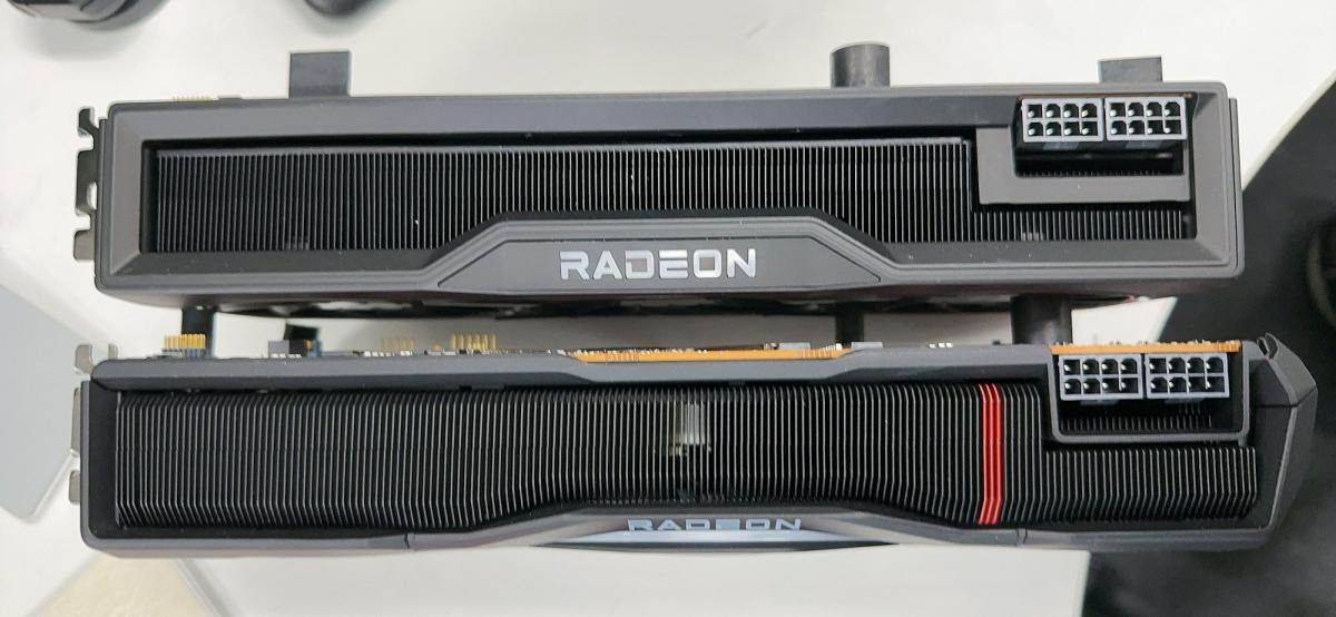
The best estimates we have right now are 1x 308mm2 of N5 Graphics Complex Die(GCD; contains the WGPs), and 6x 37.5mm2 of N6 Memory Complex Dies (MCD; these house the GDDR PHYs and the Infinity Cache/xGMI/Infinity Fabric links to the GCD)
So you're looking at a total die area of around 533mm2, compared to AD102's 608mm2.
So no not exactly a monster by any definition.
MCM is automatically gonna pull more heat compared to monolithic.
Ah so you have the engineering samples? Yes inter connects tend to draw more power, but how much power is that exactly?
MCM is going to add latency.
How does this impact GPU performance, if at all?
There aren't multiple GCDs, all of the compute is on a single die. They have simply disaggregated the Compute from the fixed function IO/Cache which doesn't scale as well. So I can't see this having a significantly negative impact. Besides, CPUs are far more latency sensitive than GPUs, and Ryzen multi-chip processors seem to handle it just fine as the core physical design has absolutely exceptional latency handling. I'm sure a lot of that expertise as cross pollinated with Radeon Technologies Group.
More chiplets, the more crossbars, the more the data has to make a jump at a node, it's the basics of NUMA topology.
Where did you get the impression that this is NUMA? Single compute die.
"B..b.. but Ryzen?" you say, CPU tasks not sensitive inter-GPM bandwidth and local data to latency like GPUs are.
GPU's are designed to hide latency way more than CPUs. GDDR memory has significantly higher latency than normal DDR. The tradeoff is higher bandwidth. That's why GPUs use high bandwidth, high latency GDDR, while CPUs use low bandwidth, low latency DDR.
AMD's MI200s and Nvidia's (2) H100 chipsets were MCM and were made for tasks with low latency requirements such as scientific computing. NVlink's 900GB/s and MI200s infinity fabric's 100GB/s per links with 8 links providing 800GB/s, are still no match for the whooping 2.5TB/s Apple made for the M1 Ultra.
Do you know what packaging technology they're using for this GPU? Because Apple is using a technology that TSMC developed - its probably pretty easy for AMD to just license that same tech if they need to have high bandwidth between dies.
That 2 chipset MCM basically had double CPU performances, while GPU had a +50% increase on their own freaking API! Because don't forget, this segmentation of tasks that are ultra sensitive to fast local packets of data such as FSR/RT/ML will have to be entirely invisible from the API's point of view and since we're on PC, it's on AMD's shoulders to make drivers for that.
Yes that is why each MCD has 16MB (or maybe more) of cache - to maintain data locality. I'm sure that will do a great deal to help handle RT and BVH structures.
What else is rumored.. oh, let's add 4GHz into the mix, 100 less watts, match or surpass a 4090 in rasterization, expensive communication crossbars that are outside of lithography but still manage -$600 over competition. Pulling performances out of a quantum parallel universe basically.
What? AMD took Navi 10, a GPU that clocked at 1900MHz on N7 and made Navi 21, a GPU that sits comfortably at 2500MHz - and is often capable of doing more like 2800MHz also on N7. They gained significant clockspeed without a node transition. So now they're moving from N7 to N5 - what is often described as a bit of a Unicorn node. Why would you think they wouldn't be able to extract similar gains in frequency yet again. I don't expect 4GHz, but certainly 3.5GHz is not outside of the realms of possibility.
Especially if the architecture has been specifically designed to clock fast by the way of its physical design. And RDNA is designed to clock high.
Prices are subject to change at the drop of a hat, so I'm not going to engage with you on the point of what people expect the prices to be. Because they're all probably wrong. However, it seems that you're just unwilling to accept that AMD might be able to engineer a more power-efficient architecture than Nvidia. The lead of Radeon; one David Wang, was a senior engineer who helped develop Cypress (of HD5870 fame) which was vastly more power efficient than Fermi way back when. Also please note that the 4090 is overvolted into oblivion. You can drop the power down to 350W and you'll barely lose 5-10% performance. They've overclocked the shit out of it out of the gate to extract as much performance as possible. Wonder why that is?
Anyway, I guess AMD don't feel the need to overclock the shite out of their GPU. If they can get close enough, say with in 10%, but at significantly less power, then that's good enough.