ethomaz
Banned
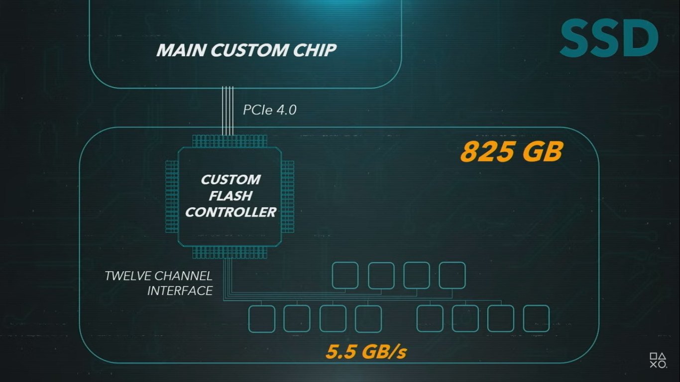
Again they didn't show the I/O controller in the teardown.The diagram is irrelevant, watch the teardown video.
It should be hard to show a part of the APU btw.
Last edited:
Again they didn't show the I/O controller in the teardown.The diagram is irrelevant, watch the teardown video.
No the I/O unit is literally a part of the APU. Thats not the SSD's flash controller. They're different.The diagram is irrelevant, watch the teardown video.
So 22mm², which we don't know what it is used for?
PS4 Pro Boost mode is just running the GPU at 911Mhz instead of 800Mhz and does not enable the use of the full GPU. As for the PS5 BC, they even have a patent describing how it works:Sony did same with ps4 pro, and every ps4 game I played ran in boost mode anyway. They just covering their arses in a litigation world.
Also Sekiro was not confimed to be using checkerboard on pro, DF could not work it out.
Anyway, whatever caps are in last gen titles for both consoles, hopefully we get patches and updates for everyone if third party play nice.

No, and it's even explicitly shown in the teardown video.

The diagram is irrelevant, watch the teardown video.
That's the custom SSD controller. Different from the IO complex inside the SoC.The diagram is irrelevant, watch the teardown video.
Okay, then it's my fault, because the I/O-Complex aka SSD-Controller is to see at 5:35 in the Teardown-Video.No the I/O unit is literally a part of the APU. Thats not the SSD's flash controller. They're different.
Yeah, series s isn't being used as remote xcloud server blades. I do wonder if series s plays into the whole distributed xcloud server play that Phil Spencer said in a e3 after hours event.To run 4 Xbox One games from 1 chip is different than to run 1 next gen Xbox game from 1 chip. I think they will use both for different uses. You're likely correct too. But the Series S chip can't run 4 One games at once, and Xcloud is mainly Xbox One games. And the stream will only need to be around 720p, so they can get the most bang for the server's buck with the X chip.
The diagram is irrelevant, watch the teardown video.
Okay, then it's my fault, because the I/O-Complex aka SSD-Controller is to see at 5:35 in the Teardown-Video.
I know how virtualization works.To run 4 Xbox One games from 1 chip is different than to run 1 next gen Xbox game from 1 chip. I think they will use both for different uses. You're likely correct too. But the Series S chip can't run 4 One games at once, and Xcloud is mainly Xbox One games. And the stream will only need to be around 720p, so they can get the most bang for the server's buck with the X chip.
Okay, then it's my fault, because the I/O-Complex aka SSD-Controller is to see at 5:35 in the Teardown-Video.

And now you're going to tell me that the flash memory controller is almost as big as the PS5 APU? Look at the Teardown, this is not a simple hard drive controller ...APU IO Complex != Flash memory controller.
Yup. Same as if the SoC or RAM dies. RIP. Or try to repair it yourself somehow.That cooling system looks pretty solid, and it was a nice touch to add a dust trap, my main worry is the fact that the main SSD is attached to the motherboard, if it stops working does that mean the PS5 is dead?
But Sony is struggling and don't know how to do marketing. Lmao
And now you're going to tell me that the flash memory controller is almost as big as the PS5 APU? Look at the Teardown, this is not a simple hard drive controller ...
I know how virtualization works.
They also can get bang for the bucks they already spent outfitting their data centers with Xbox One S blades. Just depends on what is more important to them; the space they need or the money they want to spend upgrading hardware. Throwing out old Xbox One S blades any time soon would be a huge waste considering xCloud is in it's infancy.
And now you're going to tell me that the flash memory controller is almost as big as the PS5 APU? Look at the Teardown, this is not a simple hard drive controller ...
Somebody explain the following to me:
We all assume that the PS5 will perform roughly the same as the Series X, but with reduced resolution and possibly a little less ray tracing.
For this, Sony has chosen a chip that is clocked higher, that needs better cooling, the liquid metal cooling of which took two years to develop, plus an I / O that can deliver incredible performance and all for a manufacturing price almost the same as the Series X.
Why all the effort when you could have it almost as strong or even stronger, for the same financial commitment (like Series X)?
The I/O controller?A mix of the extra I/O, infinity cache? and future AMD GPU features?
!

V.2

9TF flop number is in the official spec given by Cerny...

The chip/ASIC is part of the I/O...That is just the package, the flash controller die is the tiny part on top!
And now you're going to tell me that the flash memory controller is almost as big as the PS5 APU? Look at the Teardown, this is not a simple hard drive controller ...


John Lineman hinting again that people will be surprised by Ps5 performance "in a good way".
Where?
It actually is... a 12 lanes SSD controller.And now you're going to tell me that the flash memory controller is almost as big as the PS5 APU? Look at the Teardown, this is not a simple hard drive controller ...

We might never know really. You could be right, I'm sure they could use the S chip somehow too.I know how virtualization works.
They also can get bang for the bucks they already spent outfitting their data centers with Xbox One S blades. Just depends on what is more important to them; the space they need or the money they want to spend upgrading hardware. Throwing out old Xbox One S blades any time soon would be a huge waste considering xCloud is in it's infancy.
You might be right; maybe the next step is adding XSX for new blades and using them as 4 Xbox One's.. rather than expanding the XOS footprint.. I still think XSS partly exists for xCloud reasons.
Why do you look for things to be upset about?So, some people( guess which ones ) still have big problems :

PS5 SoC is ~25% smaller than the Series X
I mean, some may feel it's not that big of a difference when it's currently ~18% difference in GPU performance between the PS5 and Series X doesn't mean others can post false information to make that gap seem wider than it really is.www.resetera.com
Which?Cerny said at the end of this year he expected ssds to match the speeds and we already have one
To compare, this is the flash controller for the Samsung 980 Pro M2 SSD. It is its own custom design. Sony's PS5 flash controller seems to be smaller, but sitting on a larger square of circuitry or something. Maybe thats for heat. Both controllers look to have DRAM cache chips next to them, along with the 3D TLC NAND flash dies.

Where?
980 pro which yet hasn't been confirmed as compatibleWhich?
The diagram literally shows a separate controller outside of the APU, and the "i/o complex", inside the APU.The diagram is irrelevant, watch the teardown video.
Silly?
Cerny said that himself.
"The benefits of this strategy are quite large.
Running a GPU at 2 GHz was looking like an unreachable target with the old fixed frequency strategy.
With this new paradigm we're able to run way over that in fact we have to cap the GPU frequency at 2.23 GHz so that we can guarantee that the on chip logic operates properly."

Transcribe - The Road to PS5 - Mark Cerny's a deep dive into the PlayStation 5 - - The Road to Next Gen Ludens
Thank you Jim. There will be lots of chances later on this year to look at the PlayStation 5 games.Today I want to talk a bit about our goals for the PlayStation 5 hardware and how they influenced the development of the console.playstationvr.hateblo.jp
On many occasions the Controller is not made in 7nm from TSMC to save costs. I think I remember they do it in 14nm or even 24nm.To compare, this is the flash controller for the Samsung 980 Pro M2 SSD. It is its own custom design. Sony's PS5 flash controller seems to be smaller, but sitting on a larger square of circuitry or something. Maybe thats for heat. Both controllers look to have DRAM cache chips next to them, along with the 3D TLC NAND flash dies.


Yeah I saw that thread already. Mentally ill.So, some people( guess which ones ) still have big problems :

PS5 SoC is ~25% smaller than the Series X
I mean, some may feel it's not that big of a difference when it's currently ~18% difference in GPU performance between the PS5 and Series X doesn't mean others can post false information to make that gap seem wider than it really is.www.resetera.com
The I/O controller?
I think it was this
